You are currently viewing SemiWiki as a guest which gives you limited access to the site. To view blog comments and experience other SemiWiki features you must be a registered member. Registration is fast, simple, and absolutely free so please,
join our community today!
I’m an avid road bike enthusiast having just completed my 2017 goal of 13,000 miles, so follow me on Strava if you want to see the routes and photo adventures I have in Oregon. In the photo below I’m the guy in the middle with the Portland Velojersey on and we’re in a parking lot just 2 blocks away from Intel’s… Read More
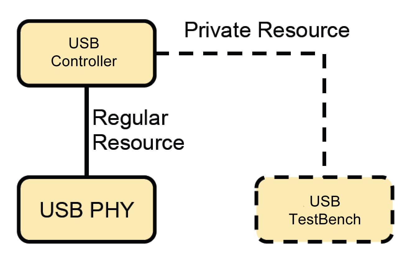
Semiconductor IP re-use is a huge part of the productivity gains in SoC designs, so instead of starting from a clean slate most chip engineers are re-using cells, blocks, modules and even sub-systems from previous designs in order to meet their schedule and stay competitive in the market place. But what happens when you intend to… Read More
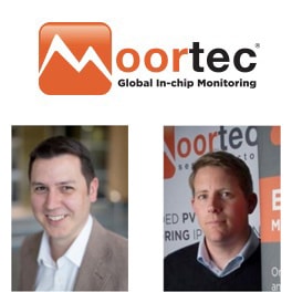
Six years ago I first interviewed Stephen Crosher, CEO and Co-founder of Moortecas they were in startup mode with some new semiconductor IP for temperature sensing, and earlier this month I attended their webinar all about embedded in-chip monitoring to get caught up with their technology and growing success. Ramsay Allen is … Read More
Our smart phone driven semiconductor economy consumes a lot of IP blocks to enable quick product development cycles, often annually updating with new models to choose from. So where do you find all of the best semiconductor IP, verification IP and embedded software? Well, one place is at the 2nd annual REUSE conference, scheduled… Read More
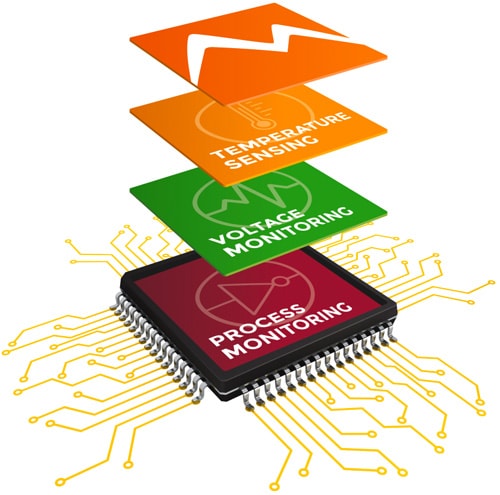
One holy grail of AI software developers is to create a system that is self-aware, or sentient. A less lofty goal than sentient AI is for chip designers to know how each specific chip responds to Process variations, Voltage levels and Temperature changes. If a design engineer knew exactly which process corner that each chip was fabricated… Read More
When I first started doing IC design back in 1978 we had hierarchical designs, and that was doing a relatively simple 16Kb DRAM chip with only 32,000 transistors using 6um (aka 6,000 nm) design rules. SoC designs today make massive use of hierarchy at all levels of IC design: IC Layout, transistor netlist, gate level netlist, RTL … Read More
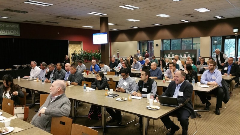
SEMI is a worldwide organization with local chapters like the one here in Oregon, where I attended a recent half-day presentation by several industry experts on the topic – Globalization, How it shapes the Semiconductor industry:
- Michael Chen, Director, Mentor – A Siemens Business
- John Brewer, CEO, Amorphyx
- Ed
…
Read More
Verification engineers are hearing a lot about the Portable Stimulus Standard (PSS), and for good reason because it could potentially save them time and effort in doing their jobs much better. In order to get the big picture on what PSS is all about I contacted Adnan Hamid, founder and CEO of Breker Verification Systems, because … Read More
I have a transistor-level IC design background so was intrigued to learn more from the CEO of an IP and services company that started out in India 12 years ago. Last week I spoke with Samir Patel, CEO of Sankalp Semiconductorabout the newest $5 million financial investment in his company from Stakeboat Capital Fund. The Stakeboat… Read More
In college I took courses in physics, calculus, chemistry and electronics on my way to earn a BSEE degree, then did an 8 year stint as a circuit designer, working at the transistor level and interacting with fab and test engineers. My next adventure was working at EDA companies in a variety of roles. As a circuit designer I knew that … Read More


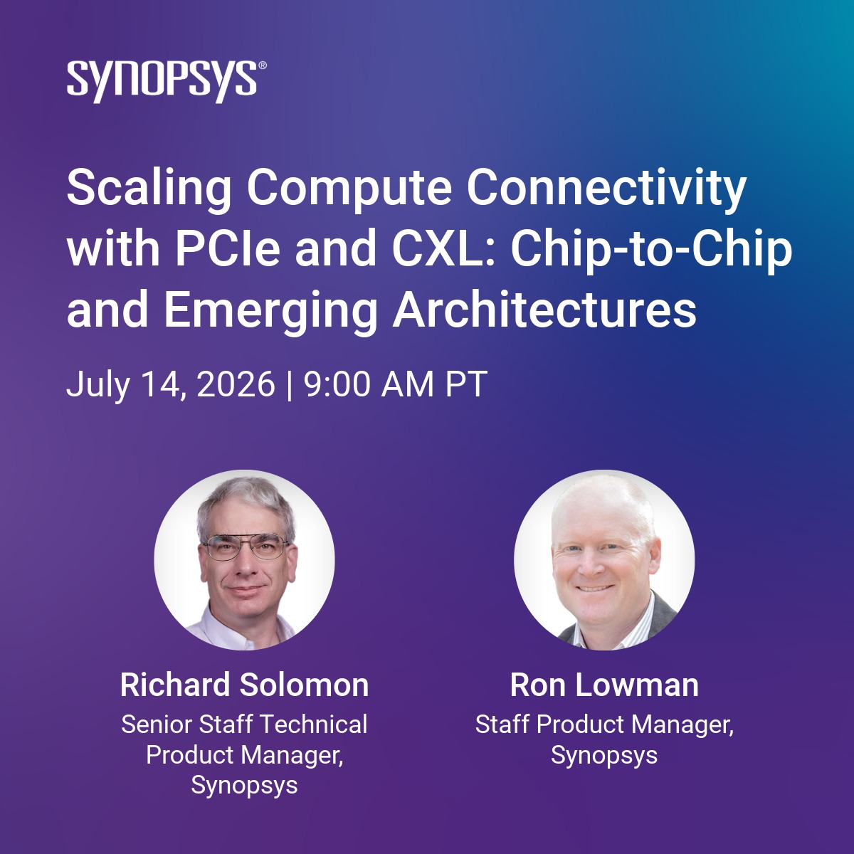


Consolidation and Competition: Who is Winning the $4.5 Billion Interface IP Race?