You are currently viewing SemiWiki as a guest which gives you limited access to the site. To view blog comments and experience other SemiWiki features you must be a registered member. Registration is fast, simple, and absolutely free so please,
join our community today!
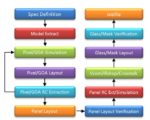
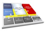
This area of automating the design of Flat Panel Displays (FPD) is so broad that it has taken me three blogs to cover all of the details, so in brief review the first two blogs were:
My final blog covers five areas:
- DRC/LVS for curvilinear layout
- Circuit
…
Read More
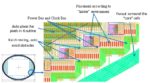
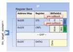
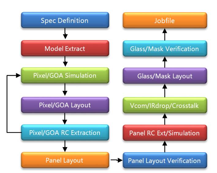
You are likely reading this blog using a Flat Panel Display (FPD), because they are so ubiquitous in our desktop, tablet and smart phone devices. Today I’m following up from a previous article. A quick recap of the unique design flow for FPD is shown below:
What follows is the second part of a Q&A discussion with Chen Zhao… Read More
Back in July I first read the news that Perforce had acquired Methodics, and wasn’t too surprised, because many of the EDA vendors that we blog about do get acquired or merge with similar sized companies in order to be part of a bigger offering. When Methodics announced a webinar introducing IPLM 3.0 (IP Lifecycle Management),… Read More
I’ve used OLED (Organic Light-Emitting Diode) displays for many years in my monitors, laptops, tablets, e-readers and smart phones; and knew that the AMOLED (Active-Matrix OLED) displays used thin-film transistor technology where each pixel can be controlled, but I hadn’t considered the actual design process… Read More
Although our family has down-sized to just one vehicle, my dream car is still a Tesla, both because it’s an EV and they have a vision for autonomous vehicles. At the recent Arm DevSummit I watched a fireside chat with Alexander Hitzinger, CEO of Artemis, the skunkworks at Audi, part of the Volkswagen Group. I knew that Audi … Read More
Oh, our semiconductor industry just loves acronyms, and the title of my blog packs three of the most popular acronyms together at once. I attended a webinar hosted by Aldec last week on this topic, “UVM Simulation-based environment for Ibex RISC-V CPU core with Google RISC-V DV“. Verification engineers have been … Read More
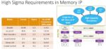
Looking at a typical SoC design today it’s likely to contain a massive amount of memory IP, like: RAM, ROM, register files. Keeping memory close to the CPU makes sense for the lowest latency and highest performance metrics, but what about process variations affecting the memory operation? At the recent DAC conference held… Read More
I’ll never forget first learning about Xilinx when they got started back in 1984, because the concept of a Field Programmable Gate Array (FPGA) was so simple and elegant, it was rows and columns of logic gates that a designer could program to perform any logic function, then connect that logic to IO pads to drive other chips … Read More
Presenters took a trip down memory lane at DAC this year by having a panel discussion on HLS (High Level Synthesis) spanning from 1974 to 2020, and that time period aligns with when I first graduated from the University of Minnesota in 1978, starting chip design at Intel, then later transitioning into EDA companies by 1986. Marilyn… Read More
DVCon was the first EDA conference in our industry impacted by the pandemic and travel restrictions in March of this year, and the organizers did a superb job of adjusting the schedule. I was able to review a DVCon tutorial called “Defining a SystemC Methodology for your Company“, given by Swaminathan Ramachandran… Read More


Captain America: Can Elon Musk Save America’s Chip Manufacturing Industry?