You are currently viewing SemiWiki as a guest which gives you limited access to the site. To view blog comments and experience other SemiWiki features you must be a registered member. Registration is fast, simple, and absolutely free so please,
join our community today!
There was some serious backlash to the “Intel Bay Trail Fail” blog I posted last week, mostly personal attacks by the spoon fed Intel faithful, but there are however some very interesting points made amongst the 30+ comments so be sure and read them when you have a chance.
The Business insider article “The iPhone… Read More
Now that the IDF 2013 euphoria is fading I would like to play devil’s advocate and make a case for why Intel is still not ready to compete in the mobile market. It was very clear from the keynotes that Intel is a chip company, always has been, always will be, and that will not get them the market share they need to be relevant in mobile electronics,… Read More
I’m looking forward to the 2013 TSMC Open Innovation Platform Ecosystem Forum to be held Oct. 1[SUP]st[/SUP] in San Jose. One paper in particular that has my attention is titled, “An Efficient and Accurate Sign-Off Simulation Methodology for High-Performance CMOS Image Sensors,” by Berkeley Design Automation & … Read More
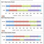
One of the benefits of blogging is that you put a stake in the ground to look back on and see how how things have changed over the years. You can also keep a win/loss record of your opinions, observations, and experiences. Last year I posted the “SemiWiki Analytics Exposed 2012” blog so here is a follow-up to that.
The Semiconductor Wiki… Read More
A good friend and dog walking partner was on the smartphone Apple/Android fence last year so I pushed him over to Apple and the result was the infamous “8 Reasons Why I Hate My iPhone5” Blog. After months of complaining I bought him a Samsung S4 and gave his iPhone5 to my very appreciative wife so all is well that ends well, maybe.
During… Read More
Ecosystem is everything when it comes to modern semiconductor design, especially if it is mobile. The fabless semiconductor industry has been all about ecosystem since the beginning and that is why we hold supercomputers in our hands today, believe it. After the invention of the transistor in 1947, and the invention of the integrated… Read More
Must See SoC IP!by Daniel Nenni on 09-02-2013 at 5:30 pmCategories: IP
IP is the center of the semiconductor universe and nobody knows this better than Design and Reuse. The D&R website was launched in 1997 targeting the emerging commercial semiconductor IP market. Today, with more than 15,000 IP/SOC product descriptions updated daily, D&R is the #1 IP site matching customer requirements… Read More
Real Heroes have many different jobs. My oldest son is a Math Teacher, he is a hero. You may have read about him before, he is the co-developer and administrator of SemiWiki. Think about it, without math where would the world be today?
My other son is a Fireman, Emergency Medical Technician, and also a hero. He is at the Rim Fire in Northern… Read More
The TSMC Open Innovation Platform® (OIP) Ecosystem Forum brings TSMC’s design ecosystem member companies together to share with our customers real-case solutions for customers’ design challenges and success stories of best practice in TSMC’s design ecosystem.
More than 90% of the attendees last year said “this… Read More
Business Insider does it again, I just love their charts and with this one I agree with the logic 100%. To me this is more about Samsung the company than Samsung products, Samsung really needs to grow up. The negative marketing, the intellectual property thefts, bribery scandals, product dumping, presidential pardons……. Is that… Read More


Chemical Origins of Environmental Modifications to MOR Lithographic Chemistry