There’s never a dull moment in the foundry race to offer FinFET processes that enable leading-edge SoC design. Today I attended a webinar hosted by Samsung and Synopsys on how to enable 14nm FinFET design. The two speakers were Dr. Kuang-Kuo Lin from Samsung and Dr. Henry Sheng from Synopsys.


Dr. Kuang-Kuo Lin, Samsung


Dr. Henry Sheng, Synopsys
Foundry, Samsung
Why FinFET?
- Lower power required for mobile devices
- 20nm planar and lower nodes are too leaky for current
- Lower VDD possible, lower power, faster switching
FinFET Challenges
- Process is more complex than planar
- Parasitic resistance goes up
- Limited device width choices, quantized
- 3D modeling and extraction is more complex than planar
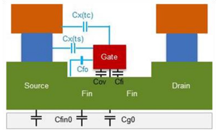
FinFET Collaboration
- Enablement (3D TCAD, parasitic extraction, SPICE modeling, early IP)
- EDA flow (FinFET ready tools, Rules and tech files, aware-models, QoR)
- Validation (Test chips, silicon correlation, early engagements, IP)
Samsung 14nm FinFET
- Samsung working on FinFET for 10 years now
- Partnered with IBM and GLOBALFOUNDRIES
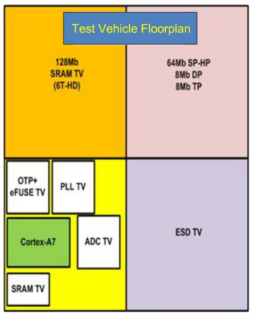
- 2012 – Test vehicle and MPW last year
- 2013 – MPW (Multi Project Wafers)
- Improved short-channel effects
- Reduced Vt mismatch (lower than 20nm and 28nm)
- 46% improvement in switching speeds, compared to 20nm
- 15% smaller die size, compared to 20nm planar
- PDK is ready, IP is ready
EDA, Synopsys
14nm collaboration with Samsung started years ago, and first test chip in December 2012 with Samsung.
20nm marked the end of planar scaling. DPT (Double Pattern Technology) is required at 20nm and lower for DFM (Design For Manufacturing).
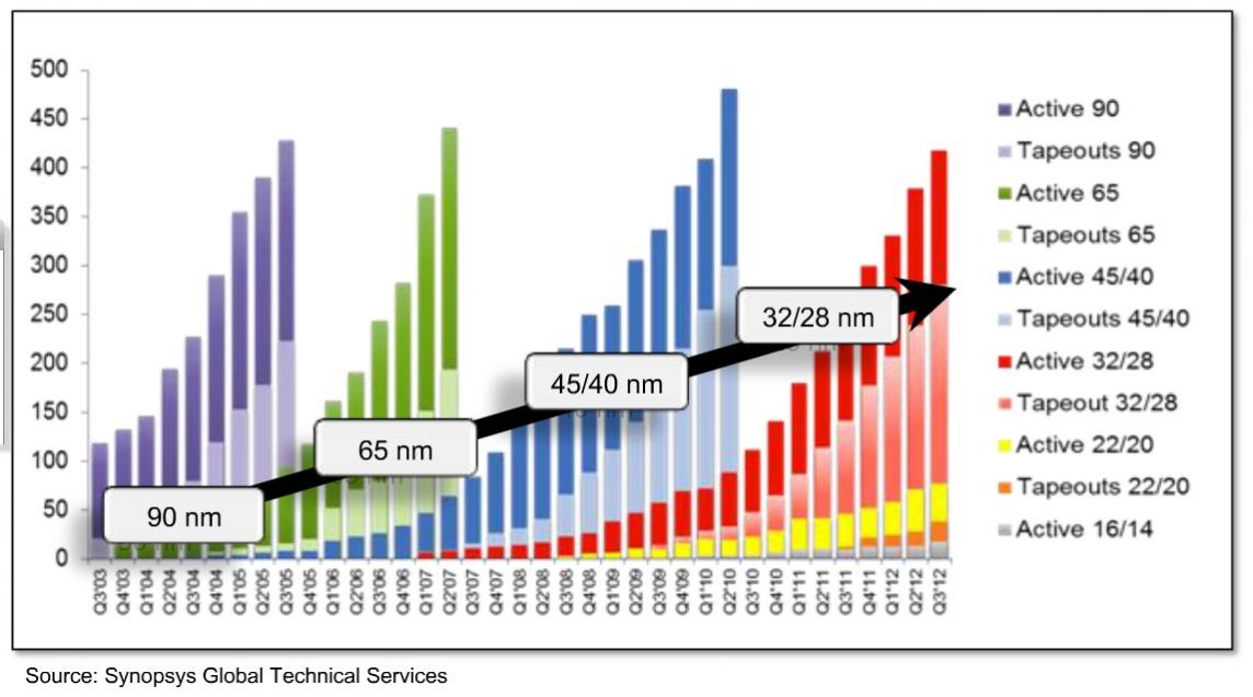
Lots of change in EDA to make tools FinFET-ready.
Goal – make the required FinFET changes almost invisible to EDA tool users.
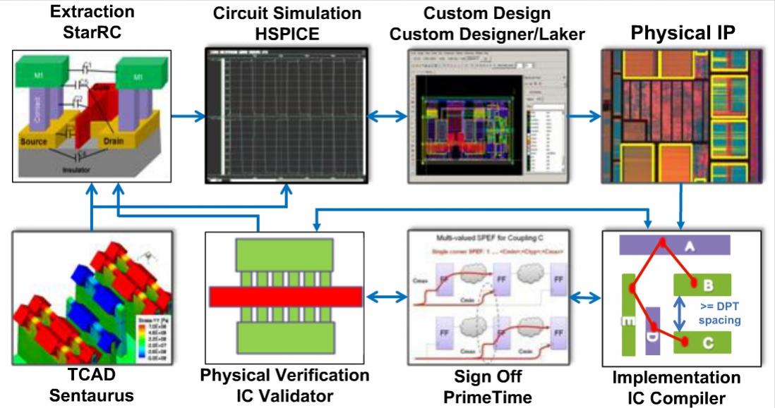
Design Challenges
- Cross section of 14nm wires is much thinner than at 65nm, so resistance goes up. Resistance is very dominant at 14nm.
- Metal stacks are bloomed, instead of same widths
- Capacitance per micron about the same
- More vias required per net
- 2-3X gate capacitance compared to planar
- Power can go up
- Electromigration (EM) issues increase
- Self-heating creates a reliability issue
- Line width/edge roughness impacts current and timing
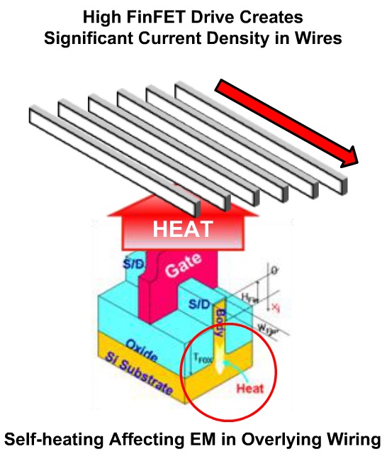
EDA tools upgraded for 14nm FinFET
- Place & Route (IC Compiler)
- Target either low Vdd or high performance to achieve specific QoR
- Dynamic power optimization, reduction of overal wire length
- Signal EM analysis
- Clock Tree Synthesis (CTS), Multisource and Clock Mesh approaches to clock assembly
- Convergent timing closure flows, cell choices must be tolerant to process variability
- Strong timing correlation between P&R with IC Compiler and PrimeTime SI, 99.92% of endpoints within 1% of PrimeTime SI
- Design Rule Checking (DRC) – IC Validator updated for 14nm FinFET technology. Call physical validation during P&R, eliminate extra work.
- Power analysis with PrimeRail (EM, Power density, dynamic voltage drop, de-cap analysis)

Questions
Q: What FinFET process node is Samsung offering today?
A: 14nm LPE is offered now, the PDK version 0.1 is ready now. Beta version available soon. Test chip taped out and analyzed. Shuttles available now. Smaller poly-pitch, smallest SRAM bit cell.
Q: With increased resistance, do we need to add more buffers?
A: Timing closure is more challenging, but we get benefit from improved drive strengths. Not really seeing a large increase in number or size of buffers. Wire optimization is helpful to optimize timing.
Q: Do we need multi-Vt at 14nm to handle leakage reductions?
A: FinFET devices in general have much better leakage performance, so we’re not using multi-Vt with FinFET.
Q: How does the collaboration work between Samsung and Synopsys?
A: We’ve been partnering for years to get 14nm FinFET working. The collaboration starts early and is proven through test chips and MPW efforts.
Q: What about IP availability at 14nm?
A: Samsung has added Synopsys interface IP, and our own standard cells and SRAM arrays.
Summary
With the 20nm node just ramping up now, it’s pretty impressive to see what Samsung and Synopsys are doing together at the 14nm node with FinFET technology. SoC design teams still have to go through a careful financial and technical analysis to determine if they really need the power, performance and area offered by 14nm compared with 20nm. It’s an exciting time to be an IC designer with so many technology choices available.
If you’re attending DAC next week in Austin then you can find Synopsys events here or visit them in Booth #947, Samsung is in Booth #915.

lang: en_US
Share this post via:


Disaggregating LLM Inference: Inside the SambaNova Intel Heterogeneous Compute Blueprint