





Why integration boundaries, assembly strategies, and manufacturing yield must be engineered together
The Shift from Optical Performance to Manufacturing Scale
Co-packaged optics (CPO) is moving beyond laboratory demonstrations toward commercial deployment in AI infrastructure. As switch bandwidth continues to increase, the electrical distance between switching silicon and optical transceivers is becoming an increasingly important constraint on power efficiency and system density.
Conventional pluggable optics require high-speed electrical signals to travel across printed circuit boards before reaching the optical module. At higher signaling rates, those paths introduce insertion loss, reflections, equalization requirements, and additional power consumption.
Bringing optical conversion closer to the switch ASIC can shorten these electrical paths and reduce the energy required to transport data.
The performance motivation is well established. Broadcom has demonstrated 51.2 Tbps CPO switching with substantial optical-interconnect power savings, while NVIDIA is advancing high-density photonics switching platforms with tightly integrated optical engines.
However, moving optics into the package changes more than electrical performance.
It changes where optical alignment must be established, when photonic components can be tested, which interfaces experience thermal and mechanical loading, and whether manufacturing defects can be corrected before expensive assemblies are completed.
The next engineering challenge is not simply achieving better optical performance. It is preserving that performance through a repeatable and economically viable manufacturing process.
This distinction becomes increasingly important as CPO transitions from successful demonstrations to sustained production.
Different Architectures, Different Engineering Priorities
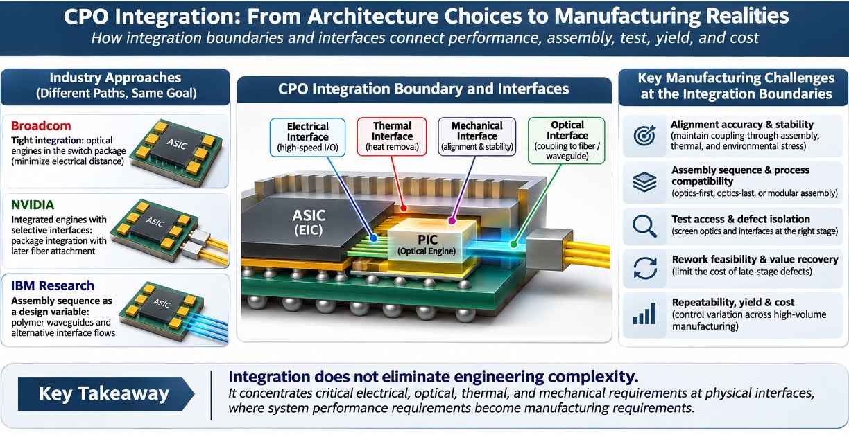
Several industry developments illustrate the range of approaches being pursued. These should not be understood as competing implementations of an identical package, but as different solutions to the same fundamental problem: integrating high-bandwidth optics with electronic systems while managing physical interfaces and manufacturing complexity.
Broadcom: Minimize the Electrical Distance
Broadcom’s Bailly CPO platform integrates eight silicon-photonics-based optical engines with a Tomahawk 5 switching ASIC, delivering 51.2 Tbps of switching capacity.
The architectural emphasis is clear. Placing the optical engines within the switching package shortens high-speed electrical connections and reduces dependence on the longer board-level paths required by conventional pluggable optics.
This integration enables significant improvements in electrical efficiency and optical bandwidth density.
But the physical architecture also moves critical manufacturing operations closer to the high-value switching silicon.
Optical-engine attachment, package-level thermal behavior, electrical connections, and fiber coupling become part of an increasingly interconnected assembly.
The manufacturing challenge is no longer limited to producing acceptable optical engines and ASICs independently. It includes maintaining acceptable performance after those components have been combined.
As integration density increases, package-level inspection, assembly stability, test access, and cumulative defect exposure become more consequential.
Broadcom’s approach illustrates the performance opportunity of tight integration and the corresponding importance of high-yield package assembly.
NVIDIA: Preserve Selected Manufacturing Interfaces
NVIDIA’s Spectrum-X Ethernet Photonics architecture demonstrates a different set of integration choices.
Its multi-chip module incorporates silicon-photonics engines attached to the package substrate through solder-reflow-compatible processes. At the same time, the design uses detachable fiber connectors that permit optical fiber attachment during a later manufacturing stage.
This distinction matters.
The optical engines remain closely integrated with the switching package, preserving the advantages of short electrical interconnections. However, fiber attachment is separated from earlier assembly operations.
That separation creates an opportunity to screen optical engines before final integration and automate fiber attachment without subjecting the fiber connection to every preceding manufacturing step.
The design therefore preserves an important assembly boundary without necessarily making the optical engines themselves independently field-replaceable.
The physical interface has not disappeared. Instead, the architecture determines when it is formed and which manufacturing operations occur before or after it.
This illustrates a broader principle: tight electrical integration and selective manufacturing modularity are not mutually exclusive.
IBM Research: Make the Assembly Sequence a Design Variable
IBM Research provides a complementary perspective through its work on polymer optical waveguides and CPO module assembly.
Its published demonstrations have evaluated different integration sequences, including attaching photonic integrated circuits to polymer waveguides before other module operations and introducing the optical interface later in the process.
The research has also examined compatibility with solder reflow and subsequent thermal and environmental reliability testing.
The significance is not that one assembly sequence universally outperforms another.
It is that optical integration can be engineered around different assembly orders, substrate geometries, and interface structures.
Polymer waveguides can provide a route between photonic devices and external fiber interfaces while introducing additional opportunities to manage optical routing density and package geometry.
But those benefits depend on adhesion, coupling loss, material stability, dimensional control, and process compatibility.
IBM’s work demonstrates that the optical interface and the sequence used to construct it must be considered together.
Unlike commercial switching platforms, these research demonstrations primarily establish technical feasibility and potential manufacturing approaches. Their broader production economics require separate validation.
Interface Challenges Push CPO Manufacturing to the Edge
The approaches pursued by Broadcom, NVIDIA, and IBM Research differ in architecture, integration sequence, and interface design. Yet they reveal a common challenge: as optical and electronic functions become more tightly integrated, the manufacturing requirements at their physical boundaries become increasingly demanding.
Each interface must satisfy its own electrical, optical, thermal, and mechanical requirements while remaining compatible with the constraints imposed by neighboring components.
Consider the placement of an optical engine near a high-performance switching ASIC.
Shorter electrical connections can reduce channel loss, equalization requirements, and power consumption. But closer integration also places the optical assembly within a more complex thermal and mechanical environment.
Higher local temperatures, package deformation, material expansion, and assembly-induced stress can affect the optical interface. The same architectural decision that improves electrical performance may therefore increase the difficulty of maintaining optical alignment and coupling efficiency.
This creates a coupled engineering problem. The electrical interface benefits from proximity, while the optical interface may require tighter dimensional control, greater thermal stability, or additional alignment capability.
The manufacturing process must satisfy both requirements simultaneously.
The challenge extends beyond the EIC–PIC connection. Fiber attachment, waveguide coupling, package substrates, cooling structures, and mechanical supports introduce additional interfaces with different sensitivity to process variation.
An assembly operation that improves one interface may disturb another. A thermal treatment that completes an electrical attachment may alter optical alignment. A mechanical structure introduced to improve stability may change the thermal environment or complicate optical test access.
Integration does not eliminate engineering complexity. It concentrates critical performance requirements at physical interfaces, where multiple constraints must be satisfied together.
This is particularly important for high-volume manufacturing. A process capable of producing one successful assembly may not consistently maintain the same relationships across manufacturing lots, equipment variations, and operating conditions.
The challenge is therefore to establish manufacturing processes that preserve the intended behavior of the complete interface system, not merely the specifications of its individual components.
Optical Alignment: Where Architecture Meets Process Capability
Optical alignment provides one of the clearest examples of this interaction.
Coupling efficiency depends on the relative position and orientation of the optical structures. Lateral displacement, vertical separation, angular misalignment, and changes in mode overlap can increase optical loss.
The sensitivity depends on the coupling architecture. Edge coupling, grating coupling, expanded-beam structures, and waveguide-based interfaces impose different requirements on placement accuracy and dimensional stability.
A successfully aligned optical engine does not necessarily remain aligned after manufacturing.
Adhesive curing can produce displacement. Thermal excursions can change package geometry. Substrate warpage and differences in thermal expansion can alter the relative positions of photonic components and fiber interfaces.
These mechanisms connect the selected integration architecture directly to the manufacturing process.
An optics-first approach must preserve alignment through subsequent assembly operations.
An optics-last approach must achieve the required alignment within an assembly whose geometry and access may already be constrained.
A detachable or modular interface must reproduce sufficient alignment accuracy each time the components are mated.
Passive alignment may improve manufacturing throughput when geometric tolerances are adequately controlled. Active alignment may compensate for selected placement errors, but requires additional equipment time and optical feedback.
Neither method independently guarantees stability after bonding, thermal cycling, or operational stress.
The manufacturing requirement is therefore not simply accurate initial placement.
It is retained optical performance after the complete assembly and operating environment have imposed their physical effects.
This distinction is essential when evaluating whether an optical integration strategy can transition from prototype assembly to high-volume manufacturing.
Manufacturing Yield Depends on Where Defects Become Visible
The economics become more complicated when multiple optical engines are integrated into one expensive switching package.
Suppose an assembly contains eight critical optical integration operations, each with a hypothetical 99% acceptance probability.
If those operations are independent and every operation must pass, the combined probability of acceptance is approximately 92.3%.
The calculation is illustrative. Actual defects may be correlated, and successful rework or redundancy can change the result.
Nevertheless, the example shows why a high acceptance rate at an individual interface does not necessarily produce equally high acceptance for the completed assembly.
Now consider when a defect is discovered.
An optical engine that fails screening before package integration can potentially be rejected without affecting the switching ASIC.
The same defect discovered only after permanent attachment may place a significantly larger assembly at risk.
A late optical-alignment failure could affect the value of the engine, substrate, ASIC-related assembly operations, thermal structures, and completed testing.
Recoverability becomes an important economic variable.
This is not an argument that every optical interface should remain detachable. Detachable interfaces introduce their own costs and reliability requirements.
Rather, the economics depend on which defects can be detected before final integration, which can be corrected afterward, and how much manufacturing value becomes unrecoverable at each stage.
An architecture with slightly more interfaces may be economically preferable if those interfaces provide meaningful independent screening or rework opportunities.
Conversely, a permanently integrated architecture may be preferable if process capability is sufficiently mature and the resulting performance and cost advantages outweigh the consequences of occasional assembly failures.
The appropriate decision depends on the actual process distributions, repair options, component costs, and production volume.
Design for Test Becomes an Architectural Requirement
CPO also changes the relationship between design-for-test (DFT) and manufacturing.
In conventional electronics, electrical probing, scan structures, and functional test techniques provide established methods for examining devices before and after packaging.
Photonic devices introduce different requirements.
Optical probing may require precise fiber or probe alignment, optical sources, wavelength control, calibrated receivers, and stable optical coupling during measurement.
Some optical characteristics can be tested at wafer level. Others become meaningful only after the EIC and PIC are integrated, external optical interfaces are attached, or operating temperatures are applied.
This makes the location of the test boundary important.
Can the PIC be characterized before EIC attachment? Can the assembled engine be screened before joining the switching package? Can optical coupling be measured before permanent fiber attachment? Can final test distinguish an electrical defect from an optical alignment defect?
The answers affect package geometry, interface accessibility, equipment requirements, and assembly sequence.
Testability therefore cannot be treated solely as an activity performed after design completion.
It must influence the architecture.
A package that provides excellent optical performance but requires difficult, slow, or poorly repeatable test access may face substantial manufacturing cost at higher production volumes.
Likewise, adding test interfaces that compromise optical performance or mechanical stability can eliminate the benefits they were intended to provide.
The practical objective is to establish sufficient test coverage at the stages where meaningful defects can be identified before additional assembly value is committed.
That requires balancing test time, measurement uncertainty, equipment utilization, defect coverage, and the cost of late-stage failures.
The Manufacturing Challenge at CPO Integration Boundaries
The performance advantages of CPO depend on bringing electronic and optical functions into closer physical relationships. But these relationships create integration boundaries that must be manufactured, inspected, tested, and preserved through the complete product lifecycle.
The manufacturing challenge begins with interface formation.
Electrical connections must satisfy signal-integrity and interconnect-reliability requirements. Optical connections must preserve coupling efficiency within the available loss budget. Mechanical attachments must maintain the necessary relative geometry, while thermal paths must support the operating conditions of the integrated system.
These requirements are not independent.
A change in attachment materials may improve mechanical stability while altering thermal resistance or cure-induced displacement. Reducing electrical interconnect length may require optical components to operate in a more demanding thermal environment. Introducing a detachable fiber interface may improve assembly flexibility while creating additional alignment and optical-loss requirements.
The integration architecture therefore determines where manufacturing precision is required and which process variations can affect multiple performance domains simultaneously.
Assembly sequence becomes especially important at these boundaries.
Optics-first integration may provide greater physical design flexibility but expose sensitive optical interfaces to subsequent processing.
Optics-last assembly may reduce some exposure but require precision attachment after the package has become mechanically and thermally constrained.
Modular optical assemblies may preserve independent screening and selected rework opportunities, but introduce interfaces that must remain stable and repeatable.
Each approach relocates manufacturing difficulty rather than eliminating it.
Test access introduces another challenge. A boundary that cannot be independently characterized may force engineers to discover interface defects only after additional high-value components have been incorporated.
Similarly, a permanently bonded interface may provide excellent operating performance but limit the ability to recover an otherwise functional assembly if the optical attachment fails.
These consequences become increasingly important as manufacturing volume grows.
The relevant measure of process capability is not simply whether each component meets its individual specifications. It is whether the integrated interfaces consistently preserve electrical, optical, thermal, and mechanical performance across representative manufacturing populations.
This requires control of dimensional variation, material behavior, process stability, interface quality, test uncertainty, and assembly-induced changes.
The engineering objective is not necessarily to minimize the number of interfaces or preserve every possible modular boundary.
It is to determine which interfaces must be permanently integrated, which can be independently assembled or tested, and how each will be manufactured with acceptable variation, yield, reliability, and cost.
The integration boundary is where system performance requirements become manufacturing requirements.
That is the critical connection between CPO architecture and its industrialization.
From Optical Performance to Manufacturable System Performance
CPO is advancing because high-performance AI networks increasingly benefit from moving optical connectivity closer to switching silicon.
Broadcom, NVIDIA, and IBM Research demonstrate different aspects of that progress: compact electrical integration, selective manufacturing interfaces, and alternative optical assembly strategies.
These developments point toward a common engineering requirement.
An optical architecture must do more than achieve excellent nominal performance. It must establish a manufacturing sequence that preserves optical alignment, supports meaningful verification, controls cumulative variation, and limits the economic consequences of defects.
The location and construction of physical interfaces determine how those requirements can be achieved.
Ultimately, the success of CPO will depend not only on the performance of the electrical and optical components, but on the ability to turn their integration into a repeatable, testable, qualified, and economically scalable manufacturing process.
Moh’s Golden Rule:
The success of CPO integration is determined not only by the performance of its components, but by the ability to manufacture and preserve the interfaces that connect them.
Also Read:
Glass Is Becoming an AI Infrastructure Platform
From 25 Million Pixels to a Six-Ounce Product: Engineering Visor for Manufacturing
AI-EDA Agents Can Prove Their Value
Share this post via:


The $725 Million Chip Development: Why Execution Risk, Not IP Cost, Now Dictates Advanced-Node Survival