
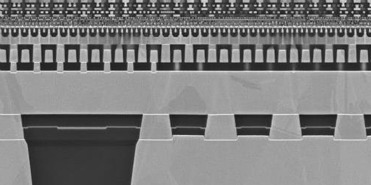
There are many threads about backside power but I am lost on a key point: when/how is the backside metal put in place?
Conventionally, a finished wafer would be ground from the backside to expose vias.
In BP, it seems to be that the power lines are laid down first and the transistors are built on top. Is that really the case? I am not understanding how the wiring could survive diffusion, implant etc. Some of these steps are very energetic and would presumably ruined the underlying metal (by allowing barrier films and metal films for example). Additionally, what kind of epi structure do you get by etching deep trenches, filling them with metal and then laying down oxide and then epi on top?
I must be missing something.

")