What does mango beer have to do with semiconductor design and manufacturing? At a table of beer drinkers from around the world I would have never thought fruity beer would pass a taste test, not even close. As it turns out, the mango beer is very good! Same goes for 20nm planar devices. “Will not work”, “Will not yield”, “Will not scale”, as it turns out 20nm is very good!!! The leading edge fabless people who were scratching their heads six months ago are now scheduling 20nm tape-outs for Q1 2013. Crowd sourcing wins again!
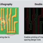
The 20nm process node represents a turning point for the electronics industry. While it brings tremendous power, performance and area advantages, it also comes with new challenges in such areas as lithography, variability, and complexity. The good news is that these become manageable challenges with 20nm-aware EDA tools when they are used within end-to-end, integrated design flows based on a “prevent, analyze, and optimize” methodology.
I agree with this statement 100%. It comes from a Cadence white paper A Call to Action: How 20nm Will Change IC Design. 20nm was definitely a turning point for the semiconductor ecosystem. Now that the technical wrinkles have been ironed out let’s look at how the fabless business model has evolved.
“There is no doubt we are at a crossroads at the most advanced process technology nodes. In order to take positive steps forward, significant monetary and collaborative investments and resources are required from both the manufacturing and design sides of the equation,” said Ana Hunter, vice president of Samsung’s North American foundry services.
I spoke with Ana before I left for Taiwan. We are in agreement: The industry is at an inflection point and the business model is changing. A simulated IDM environment is required for fabless semiconductor companies to be competitive at the advanced process nodes, absolutely. Check out the new Samsung “Best of Both Worlds: IDM and Pure-Play Foundry” brochure.
Before, during, and after DAC 2012 I asked various engineers from the top fabless semiconductor companies what has changed for them in regards to how they work with the foundries on new process technologies. I also asked the foundries. The IDM-like answers did not surprise me since working with EDA and IP companies on new process nodes is what I do during the day. It may however surprise others who are on the sidelines and believe the latest Intel PR nonsense.
UMC actually pioneered this simulated IDM environment with Xilinx from .25 micron to 40nm. Xilinx employees literally consumed an entire floor of UMC HQ for more than a decade and acted as the dutiful wife delivering many new processes. After the Xilinx 40nm divorce, UMC is no longer monogamous and now has multiple process development mistresses including TI, Qualcomm, and IBM.
TSMC took a different approach which many people overlook. The early days of collaboration started with Reference Flow 1.0 which is now version 12.0 with many new sub flows to be rolled out at TSMC OIP in October. This collaboration included both established and emerging semiconductor and EDA companies. Next came the IP effort with TSMC developing physical IP for reference and production at zero cost to customers. Commercial IP was next with the TSMC “silicon proven” program. IP companies big and small completed an exhaustive qualification program to make it into the TSMC IP catalog. Next came the TSMC “Early Access Program” where a select group of customers and partners were included in process development activities. Correct me if I’m wrong but I believe this started at 90nm. The qualification process for Early Access was also daunting but clearly it was critical to the evolution of the fabless semiconductor ecosystem. The result being the TSMC DTP (Design Technology Platform) Division which employs hundreds of people and has spent hundreds of millions of dollars (my guess) building the industry leading “Simulated IDM platform” you see today!
That brings us to 40nm. At 28nm and even more so at 20nm the fabless people have taken up residence in Hsinchu and the foundry people have “Early Access” to the top fabless companies. Bottom line: you will be hard pressed to differentiate between a Qualcomm, Broadcom, Nvidia, or Xilinx and a modern day IDM, except of course for the actual ownership of the manufacturing equipment. And lets not forget, the now fabless TI, AMD, Fujitsu, LSI Logic and others used to be IDMs, right?
Thank you again UMC and TSMC for leading the way!