Bronco Webinar 800x100 1

Toshiba Corp. has cancelled plans to sell (ARM-based processor) computers …bad news for Toshiba, TI and the end user

Toshiba Corp. has cancelled plans to sell (ARM-based processor) computers …bad news for Toshiba, TI and the end user
by Eric Esteve on 08-31-2012 at 11:55 am

This news announced two weeks ago is not really good news for those expecting to see this new generation of computers, running Windows RT OS and no more based on x86 processor but on ARM CPU core, coming on the market. The reason invoked by Toshiba was “delays in getting adequate supplies of components” and, even if Toshiba did not specifically mention the guilty supplier, it appears that the computer was based on OMAP platform from Texas Instruments, the chip being manufactured on TSMC 28nm technology. Let’s make it clear from the beginning, this blog is not aiming at putting shame on a specific and respected chip maker like TI, neither on the largest and well respected Silicon foundry (TSMC), but rather to bring my point of view about the probably needed evolution in the Foundry/Fabless/Fab-lite equation.

At one extremity of the SC landscape, we find Intel, still undisputed leader with $54 billion revenue in 2011, being the perfect Integrated Device Manufacturer (IDM) example. That means that Intel manufacture in the company wafer fab the IC designed by Intel engineers and, by the way, using the CPU core 100% owned by the company, the x86 family. At the other extremity, we find the many “fabless” companies, which can be small start-up –in this case the fabless business model is the only way to start a SC company, due to the huge cost ($5 billion) and long delays (3 years minimum) you need to build a fab to manufacture in advanced technology nodes like 28 or 22nm- but also companies reaching revenue level of several $ billion, a well known example being Qualcomm (the company has never built any fab), but also AMD (CEO and founder Jerry sanders use to say in the 70’s that “real men have fabs”) since the company has sold the fabs to a consortium creating GlobalFoundries. In this case, the picture is crystal clear, you own a wafer fab to manufacture your chips or not.

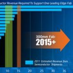
But, since the late 1990’s, the “fab-lite” concept has appeared, mainly due to the already high cost associated with the development of new technology and wafer fab equipment, very capital hungry; mainly, but not only, as the other reason is an economic theory which consider that a company should focus on core business. This theory works well for companies who have so much diversified their products that they can’t invest in every product line enough cash to be part of the leaders, this lack of leadership leading to poor capital ROI or even bankrupt. But that we are seeing these days, the Qualcomm, TI or Nvidia being unable to supply IC in 28nm at the level demanded by their customers, is showing the limits of this “MBA type” of thinking.

What can be worse than not being able to supply your flagship product (this one developed in the most aggressive technology node), offering you the best gross Profit Margin (GPM) and to your customers the best supported feature list at the lowest price and lower power consumption?

Because we are working in a fast moving industry, the first reaction have raised quickly. One option is proposed by Mike Noonen, Executive Vice President, Worldwide Marketing and Sales, for GLOBALFOUNDRIES:

“There are warning signs, both technical and economic, emerging in the foundry business that warrant our attention, and in fact require a re-thinking of how best to apply our resources and energy. The solution, ironically, may be a move toward a more IDM-like model. Strategic collaboration that creates a ‘virtual IDM-like interface’ to chip design companies will help further close the gap between process teams at the manufacturing companies and design teams at the fabless companies. Collaboration – early, often and deep – is really the only practical approach given the cost and complexities involved.”

Mike Noonen is Executive Vice President, Worldwide Marketing and Sales, for GLOBALFOUNDRIES. In this role, he is responsible for global customer relationships as well as all marketing, sales, customer engineering and quality functions.You can find his blog on GFI or ARMweb site.

This is not the only option, and I consider we should also think to another solution, which is for a fab-lite company to carefully select which product to fab outside. This remind me a meeting I had in 2005 in Shanghai with one of the SMIC Director, who share with me how this pretty young foundry did to grow so fast. At that time, SMIC business model was to build fabs, using their customer money, and manufacture the mature products for the TI and Motorola, so probably on 250 or 180nm at that time. We could imagine that the IDM going Fab-lite decide that their core business should include wafer fab, as far as these will be used to manufacture their flagship products, most often in the most advanced technology nodes. This should not prevent them to work with foundries, either for mature products, either to add extra capacity on these flagship products when the market demand is passing a certain level, or even to get better cost from foundries…

The risk is to stay in current situation, and not taking any of these decisions. Risk for these pure fabless or fab-lite IDM to miss the market window on high runner SoC for smartphone or media tablet, and get weaker, and risk also for us, the consumer, the be locked to Intel processor based only solution, when we see the opportunity to buy ARM based media tablet running on Windows RT operating system vanishing, because of wafer fab capacity issue.

Eric Esteve from IPNEST


Arteris joins Inc. 500 List of America’s Fastest-Growing Private Companies… thanks to Arteris customers!

Arteris joins Inc. 500 List of America’s Fastest-Growing Private Companies… thanks to Arteris customers!
by Eric Esteve on 08-31-2012 at 4:35 am

Arteris, founded in 2003, is the inventor and leading supplier of network-on-chip (NoC) interconnect IP solutions. Can we say that the company is still a start-up? I would say yes, as their flagship product, FlexNoc (Network on Chip IP function) was a completely new concept when it was introduced. As for every disruptive technology, it takes time for the new concept to be, at first understood by the potential customers, then tested and evaluated, and finally sold. I would say yes as well when looking at the 2011 to 2010 year to year growth rate of 115%. Sales of Arteris’ unique FlexNoC IP product have driven the growth of the company as Arteris’ patented NoC technology displaces older interconnect technologies such as hybrid busses, tiered switches and crossbars.

So, the Arteris start-up has joined the Inc. 500 list of America’s fastest growing private companies, and this is good news for the SC industry: it means that it is still possible to start an IP company, based on real innovation, and finally be successful. As a side remark for our venture capital friends, please note that it took some time (9 years), and that the company is still in pre IPO stage… it takes some time to cook a good recipe, but the result is far better than fast food (at least according with my French taste).

We have talked in Semiwiki about Arteris product port-folio, including FlexNoc, MIPI LLI (Low Latency Interface) and C2C (Chip-To-Chip Link), so it could be a good idea to look at what has made the success of the company, I mean Arteris’ customers. When you say NoC, you think SoC, and you almost immediately link SoC to Application Processor for smartphone and media tablet, which is true, but we will see that Arteris’ customers develop SoC targeting many other market segment: Video Processing, Consumer Electronics, Automotive, Networking, Multimedia (digital TV), even if a majority develop Application Processor SoC. Let’s start with these:

As you can see, most of the leaders in Application Processor SoC have selected Arteris, and they are located in the USA, Korea and China. OK, Intel is missing on this list, but the success of Intel as a low power chip maker for Application Processor is still to be demonstrated…

Another market segment where Arteris FlexNoC seems to be very popular is Video and Imaging, and the company enjoys design-in with many companies, once again located in various places like USA, Japan, Korea or India:

Because the SoC developed for Consumer Electronics are probably the most complexes, integrating an IP count which can be above 100 (SoC for the Set-Top-Box, for example), developed on one technology nodes just behind the Application Processor, integrating a Network-on-Chip is an obvious solution to speed up the Time-To-Market, so we should not be surprised to see a long customer list in this segment:

This should not be a surprise to see some of the customers listed in the Application Processor segment to appear also in this list. This is not a way to count the same chip twice and increase the customer list, but reflects the fact that companies who have made the huge investment needed to develop an Application Processor are very happy to increase the ROI by targeting other segments, close in term of application (Video, Imaging…) so they can minimize the new investment by designing derivatives chips from the initial Application Processor, leading to a different implementation of the NoC IP. If you look for example at OMAP platform from TI, you will notice various chips named OMAP4XX, each of them targeting a specific segment from Automotive to Wireless and Media tablet (or will be positioned from the high range to the most economical solution in the same segment).

Clearly, this long list of (prestigious) customers has made the success of Arteris. But this success has been made possible because Arteris’ unique FlexNoC NoC interconnect IP product was filling a need in the SC industry. According to the March 23, 2012 Gartner Research report, “Market Share: Semiconductor Design Intellectual Property, Worldwide, 2011”, by Gartner analysts Ganesh Ramamoorthy and Masatsune Yamaji, Arteris charted a 115% increase in IP license revenue in from 2010 to 2011. “Infrastructure IP was the fastest growing semiconductor design IP market after microprocessor IP in the past year. Its growth is correlated with the growing demand for interconnect functionality in advanced system-on-chip designs,” said Ganesh Ramamoorthy, research director at Gartner. “The increasing interconnect requirements of SoC vendors is driving the demand for network on chip technology provided by IP companies.”

Let’s give the last word to Charles Janac, President and CEO of Arteris:
“We are very excited to be named to the Inc. 500 list,” said K. Charles Janac, President and CEO of Arteris. “Since our founding in 2003, Arteris has charted our own path by continually delivering unique network-on-chip interconnect IP technology to the market. The fact that our fast growth and rapid adoption by leading companies such as Samsung, Qualcomm and Texas Instruments has occurred during challenging economic times proves that our FlexNoC IP saves our customers money, and helps them earn more revenue from their SoCs. Our internal data, based on customer experience, shows a 10x return on investment (ROI) when using Arteris IP for advanced SoC designs. This ROI results from cost savings, schedule savings, and increased SoC revenue due to better SoC performance.”

Eric Esteve from IPNEST


Did Qualcomm and Apple Attempt to Bribe TSMC?

Did Qualcomm and Apple Attempt to Bribe TSMC?
by Daniel Nenni on 08-30-2012 at 7:45 pm

It’s amazing how these rumors start and go viral. People are literally laughing here in Taiwan. I remember I wrote something that I thought was obviously satire and less than a week later someone repeated it back to me as fact since they “read it on the internet somewhere.”

According to Bloomberg: Apple Inc. (AAPL) and Qualcomm Inc. (QCOM) were rebuffed in separate attempts to invest cash with Taiwan Semiconductor Manufacturing Co. (2330) in a bid to secure exclusive access to smartphone chips, people with knowledge of the matter said.

Both proposals included investments, each of more than $1 billion, for the world’s largest custom maker of chips to set aside production dedicated to making chips exclusively for them, said the people, who declined to be identified because the details are not public.

Sounds like a bribe to me. No wonder why they don’t want to be identified. Dozens of variations have spawned from this rumor so now it is an “internet fact”:

TSMC Spurns Apple, Qualcomm Bids for Guaranteed Fab Capacity
PC Magazine

Apple, Qualcomm failed to buy TSMC chip exclusive rights [report]
ZDNet
Apple, Qualcomm won’t get to hog TSMC chip fab capacity
Ars Technica

TSMC Doesn’t Want Apple, Qualcomm’s Money for VIP Chip Access
DailyTech

Money can’t buy everything: TSMC denied Apple exclusive mobile chips acces
GigaOM

Apple, Qualcomm tried to purchase exclusive access to TSMC chip production
tuaw.com

TSMC rejected billions from Apple and Qualcomm for exclusive access
Inquirer

Semiconductor Producer TSMC Turns Down Bids From Apple, Qualcomm
the Mac Observer

Even IEEE Spectrum got in on it: TSMC’s Morris Chang Says No to Apple, Qualcomm

Would TSMC build fabs for Qualcomm and Apple? Of course, if it was a responsible thing to do for the TSMC stakeholders. Samsung already does that for Apple as an example. Would TSMC accept money from a customer for preferential treatment? Of course not, and anybody who thinks otherwise does not know TSMC or how the fabless semiconductor ecosystem works. And I can assure you that Qualcomm and Apple know.

From the TSMC website:

Our mission is to be the trusted technology and capacity provider of the global logic IC industry for years to come.

Now lets look at the authors of the rumor: Tim Culpan, Ian King, Adam Santariano. Sorry, never heard of them and not an ounce of actual semiconductor experience between them. Just my opinion of course.


Smart mobile SoCs: Made in China

Smart mobile SoCs: Made in China
by Don Dingee on 08-29-2012 at 2:00 pm

One of the comments to previous installments of this series was that there isn’t much left for the merchant suppliers of smart mobile SoCs, considering Apple and Samsung have majority share and design their own parts. The theory is this makes it hard for many suppliers to continue investing at the resource levels needed to bring a complex SoC to market.

Unless, the market we’re talking about is China. Continue reading “Smart mobile SoCs: Made in China”


Mixed-Signal Methodology Guide

Mixed-Signal Methodology Guide
by Daniel Payne on 08-29-2012 at 11:14 am

Last week I reviewed Chapter 1 in the new book: Mixed-Signal Methodology Guide, and today I finish up my review of Chapters 2 through 11. You can read the entire book chapter by chapter, or just jump directly to the chapters most related to your design role or project needs. With multiple authors I was impressed with the wide range of AMS topics they were able to cover from theory to practice. The last sentence in this blog contains a free offer. Continue reading “Mixed-Signal Methodology Guide”


Mixed-Signal Methodology Guide

Mixed-Signal Methodology Guide
by Daniel Payne on 08-29-2012 at 11:14 am

Last week I reviewed Chapter 1 in the new book: Mixed-Signal Methodology Guide, and today I finish up my review of Chapters 2 through 11. You can read the entire book chapter by chapter, or just jump directly to the chapters most related to your design role or project needs. With multiple authors I was impressed with the wide range of AMS topics they were able to cover from theory to practice. The last sentence in this blog contains a free offer, and you can enter to win a free book here.

Chapter 2: Overview of Mixed-signal Design Methodologies
The AMS methodology you choose really depends on what you are designing, so there is no single flow that fits all design styles. Approaches can be top-down, bottom-up, or meet in the middle. There’s a continuum of AMS designs from Analog-centric to Digital-centric.

Historically there were two sets of EDA tools and databases for AMS design: Analog, and Digital. Today however there are common databases and tools for IC design that allow concurrent AMS design.

Based on the amount of Analog or Digital in your design you can choose the appropriate design methodology:

Chapter 3: AMS Behavioral Modeling
SPICE circuit simulation can be used on any transistor-level netlist to predict the analog behavior of blocks of your design however at the expense of long run times. If you were to write a behavioral model of your analog block then it could simulate orders of magnitude faster than SPICE. This chapter has plenty of examples on how to start writing AMS behavioral models:

  • Programmable Gain Amplifier (Verilog-AMS)
  • Analog PGA (Verilog-A)
  • Real PGA Model
  • Digital PGA Model
  • Operational Amplifier (Verilog-A)
  • Digital to Analog Converter (Verilog-AMS)
  • Low-pass filter (Verilog-AMS)

The concept of Real Number Modeling (RNM) is introduced as a method for analog voltages to be represented as a time-varying sequence of real values.

Chapter 4: Mixed-Signal Verification Methodology
At 72 pages this is the longest chapter in the book and reflects that verification consumes more development time and engineering effort than does AMS design, just like in Digital designs. Simulation is the primary tool used to verify an AMS design, unlike in digital where you also have formal methods and Static Timing Analysis.

Assertions are being used in AMS tool flows to capture design intent and report violations. The UVM-MS (Universal Verification Methodology – Mixed Signal) approach offers a direction for a metric-driven verification. Examples of using PSL (Property Specification Language) with Verilog-AMS show how analog events for assertion clocking can be coded.

SystemVerilog Assertions (SVA) are also demonstrated by a mixed-signal Sigma Delta ADC example. Mixed-signal coverage is defined along with mixed-signal metric-driven verification, so engineers can start to measure the effectiveness of their AMS verification.

The Common Power Format (CPF) syntax is used to show how power domains are modeled and the challenges of designing for low power in mixed-signal chips.

Chapter 5: A Practical Methodology for Verifying RF Chips
Jess Chen from Qualcomm wrote a math-filled chapter showing how to verify a direct conversion wireless OFDM link. His SystemVerilog code implements a low noise passband amplifier, IQ modulator, IQ demodulator and baseband amplifier.

Simulation waveforms called Pretzels show the behavior of the RF models:

Chapter 6: Event-Driven Time-Domain Behavioral Modeling of Phase-Locked Loops
Verilog-A and Verilog-AMS was used to model a PLL circuit by decomposing the design into several blocks:

  • Phase Detector
  • Charge Pump
  • Loop Filter
  • Voltage-Controlled Oscillator

Refinements are shown that add jitter and frequency slewing for a PLL. The benefit of the behavioral model is that you can simulate PLL lock time in seconds instead of using SPICE and having to wait up to a week for results.

Chapter 7: Verifying Digitally-Assisted Analog Designs
The concept of using digital circuits to tune an analog block is gaining use, and Art Schaldenbrand from Cadence provides several examples with calibration to show a new verification methodology:


  • VCO with calibration
  • Multi-Bit Delta-Sigma ADS with dynamic element matching
  • Active-RC filter

Chapter 8: Mixed Signal Physical Implementation Methodology
Two IC layout flows are highlighted: Custom Design, and Constraint-driven.

The constraint-driven flow uses Pcells (or Pycells if you prefer non-Cadence tools) to introduce more automation and allow for process migration of analog blocks. The idea is to quickly get from schematic to layout, then use the parasitics from layout back in simulation where performance can be measured and then transistors either re-sized or layout changed.

Physical verification is also touched on:

  • LVS (Layout versus schematic)
  • DRC (Design Rule Checking)
  • ERC (Electrical Rule Checking)
  • DFM (Design For Manufacturing)

Chapter 9: Electrically-Aware Design Methodologies for Advanced Process Nodes
Layout Dependent Effects (LDE) can dominate the performance of an AMS design at 28nm and lower process nodes, so using an electrically-aware design methodology can reduce iterations and minimize design time.

During IC layout the EAD flow will take into account several LDE effects that impact variability and performance:

  • Shallow Trench Isolation (STI)
  • Well Proximity Effects (WPE)
  • Length of Diffusion (LOD)

Reliability concerns like Electromigration (EM) can be analyzed while doing IC layout, instead of waiting for final block assembly.

Chapter 10: IC Package Co-Design for Mixed Signal System
Taranjit Kukal of Cadence wrote about System in Package (SiP) as a way to integrate multiple dies with discrete components into a single package. Our smart phones are probably the most successful example of SiP technology in use today. Multiple ways of implementing SiP were shown:

  • Single die in package
  • Multi Chip Module (MCM)
  • RF module
  • 2.5D IC
  • 3D IC
  • 3D Package

Co-design between package and SiP allows for trade-off analysis early in the system design process, optimized I/O locations, and Power Delivery Network (PDN) analysis.

Chapter 11: Data Management for Mixed-Signal Designs
Michael Henrie and Srinath Anantharaman from ClioSoft described how Design Management (DM) of ICs is different than Software Configuration Management (SCM) because of the broad spectrum of design data:

  • Specifications
  • HDL design files
  • Verification test benches
  • Timing and power analysis
  • Synthesis constraints
  • Place & Route
  • Parasitic Extraction
  • Standard Cells
  • Analog Design
  • PDK (Process Design Kits)
  • Custom Layout
  • GDS II
  • Packaging
  • Scripts & Customizations

An AMS design management system should enable:

  • Collaboration across team members
  • Version control
  • Release management
  • Variant development
  • Security and access control
  • Audit trail of changes
  • Integration with bug tracking
  • Design flow integration
  • Checkin / Checkout to control access to cells, blocks and modules
  • Quick response, low disk space use
  • Composite design objects
  • Shared workspaces
  • Visual change analysis
  • Hierarchical design
  • Reuse of PDKs

ClioSoft offers one of a few DM tools that work within the Cadence environment and operates on the concept of a repository:

A DM methodology can enable an AMS team to collaborate efficiently, avoid mistakes of data loss, automate version control, analysis changes visually, plus use IP and PDKs across the organization.

Summary
Even if you are a specialist in AMS design and verification you will benefit from the big picture presented in this new book: Mixed-Signal Methodology Guide. The eleven chapters cover a wide range of relevant topics, plus there are ample references to allow you to further explore a topic. I enjoyed the numerous examples provided and code snippets as a way to learn.

As a reward for those who read this blog to the very end I am offering a free copy of the book to the first two people who post a comment and request their copy.

Also Read

Book Review: Mixed-Signal Methodology guide

Interview with Brien Anderson, CAD Engineer

Managing Differences with Schematic-based IC design


TSMC 28nm Update Q3 2012!

TSMC 28nm Update Q3 2012!
by Daniel Nenni on 08-28-2012 at 7:30 pm

Reports out of Taiwan (I’m in Hsinchu this week) have TSMC more than doubling 28nm wafer output in Q3 2012 due to yield improvements and capacity increases while only spending $3.6B of the $8.5B forecasted CAPEX! Current estimates have TSMC 28nm capacity at 100,000 300mm wafers (+/- 10%) per month versus 25,000 wafers reported in the second quarter. Wow! Talk about a process ramp! As I mentioned before, 28nm will be the most profitable process node the fabless semiconductor industry may ever see!

Continue reading “TSMC 28nm Update Q3 2012!”


Assertion Synthesis

Assertion Synthesis
by Paul McLellan on 08-28-2012 at 2:46 pm

In June, Atrenta acquired NextOp, the leader in assertion synthesis. So what is it?

Depending on who you ask, verification is a huge fraction, 60-80%, of the cost of an SoC design, so obviously any technology that can reduce the cost of verification has a major impact on the overall cost and schedule of a design. At a high-level, verification is checking that the RTL corresponds to the specification. So it follows that without an adequate specification the debugging cycle will just drag out and the design and verification teams will be unable to have confidence that there are no bugs that will cause the chip to fail.


Assertion-based verification helps teams using simulation, formal verification and emulation methodologies, to accelerate verification sign-off. The RTL and test specifications are enhanced to include assertions and functional coverage properties. These are statements that define the intended behavior of signals in the design. Assertion synthesis automates the manual process of creating adequate assertions and functional coverage properties and so makes assertion-based verification more practical.

Modern verification includes a mixture of directed simulation, constrained random simulation, formal verification and emulation. Directed simulation, where the output is explicitly tested for each feature, does not scale for large designs. Constrained random, where an external checker model of the design is used and the output of the RTL checked against the checker, suffers from incompleteness of the checker (since it is so hard to write). Assertion-based verification enhances all these approaches, supplementing the existing checkers with assertions about the internal logic. They thus inject observability into the RTL code. Often features that are hard to verify only looking at the outputs of the RTL are often easy to check using assertions about the internals.

But the challenge of assertion-based verification is creating enough assertions when they must be created manually. Generally one assertion is needed for every 10 to 100 lines of RTL code but it can take hours to create, debug and maintain each assertion. Assertion synthesis is technology that automatically creates high quality assertions to capture design constraints and specifications, and creates functional coverage properties that expose holes in the testbench.


Here’s how it works. Engineers use the RTL and test information as input to BugScope, which automatically generates properties that are guaranteed to hold for the given stimulus set. The new coverage properties provide evidence of holes the the verification does not cover, and the assertions provide observability into each blocks targeted behavior, which, if triggered, indicate design bugs. The assertions are then used with verification tools such as simulators, formal verification engines and emulation. Additional stimulus can be generated to patch coverage holes.

As these steps are repeated, the number of coverage properties (indicating holes in coverage) will decrease and, at verification sign-off, will have been replaced exclusively by assertions.

The Atrenta whitepaper on Assertion Synthesis, which includes more detail and a case-study, is here.


Power, Signal, Thermal and EMI signoff

Power, Signal, Thermal and EMI signoff
by Paul McLellan on 08-28-2012 at 1:55 pm

Increasingly the challenge with SoCs, especially for mobile, is not getting the performance high enough but doing so in a power-efficient manner. Handheld devices running multiple apps need high-speed processors that consume extremely low levels of power both in operating and standby modes. In the server farm, the limit is often getting power into the datacenter and getting the heat out again, and so even in the highest performance part of the market, energy efficiency is paramount. In addition, electronic systems are now subject to regulatory and design requirements such as EMI emission guidelines and surviving ESD tests.

All of this, of course, in an environment where chip area remains important since it drives both cost and form-factor (important especially for mobile where the devices are physically small and so components need to be small too). But there is more to cost than chip area. For example minimizing the package cost and not using the minimal amount of decoupling capacitance.

Optimizing all these conflicting requirements simultaneously requires a more inclusive multi-physics approach, and not doing domain specific (the chip, the package, the board) design and analysis. This is what Apache call chip-package-system or CPS.

The biggest bang for the buck in terms of reducing power is to reduce the supply voltage. But supply voltages are now getting close the the threshold voltage of the transistors which means that the noise margin to keep everything functional shrinks. In addition, in standby mode, we need to control the amount of sub-threshold leakage. This all puts a lot of pressure on keeping the power supply clean all the way from the regulators, through the PCB in through the package and around the power grid on the chip. This is the power delivery network, or PDN. To ensure reliably power, the whole PDN needs to be optimized and validated together.

For high performance designs, thermal analysis is another important aspect of the design. For very high performance designs, such as servers, there may be heat sinks and fans that affect the overall cost of the design. For lower performance designs where the system is physically small, such as a smartphone, there are obviously no fans. But heat dissipation and the thermal analysis that goes along with it is a challenge. The transistors on the chip are affected by temperature and so it is not just a reliability issue but it can be a performance issue too. So integrated thermal analysis of chip, package and system becomes a necessary design step.

Apache has a good overview of all these issues in their white paper on Chip-Package-PCB Design Convergence. This is just one of the white papers that have been pulled together into a microsite that brings together all Apache’s material to do with CPS, including the CPS User Group. The Apache CPS micro-site is here.


Apple’s Victory Will Re-Shuffle the Semi Industry

Apple’s Victory Will Re-Shuffle the Semi Industry
by Ed McKernan on 08-27-2012 at 2:00 pm

Apple’s legal victory over Samsung has been analyzed in thousands of articles and TWEETs since last Friday’s announcement and surely more will follow. Most of the commentary has focused on the first order impact to handset manufacturers. It is not entirely clear how it will all settle but there are sure to be secondary ramifications for Semiconductor Suppliers as it becomes the top discussion in the Executive Suites at Microsoft, Intel, Qualcomm, Broadcom, nVidia and others. A great shift in strategy might take place that until now no one could have foreseen.

Apple’s legal war is in its early stages and the victory over Samsung is likely to be followed by action against other other Android Vendors. Along with the legal war will be a FUD (Fear Uncertainty and Doubt) Campaign as Apple executives send an army of well trained lawyers to their competitors doorstep with a message that it is time to square accounts with a long term, stiff royalty contract or vacate the Andorid ecosystem. What are the alternatives for handset vendors?

Apple knows it can extract higher payments from the handset vendors than from Google, because in the end Android is FREE and handsets are not. Furthermore, handset makers are working off margins that are not as tight as PCs but are trending that way over time. A carefully structured royalty strategy will put some out of business and consolidate the industry around a few players. Samsung was target #1 because they were the largest supplier of smartphones and the favorite of Carriers looking for a low cost alternative to selling Apple.

In the near term we should expect that handset makers will turn their attention to Microsoft O/S based Smartphones. Handset makers are in a quandary though because they don’t know if they will be skinned by Apple and when the skinning takes place. Whether it is a hefty Royalty agreement or a Microsoft O/S Tax, the result in both cases will be significant in terms of a cost adder.

I look for Intel to step in and be a larger supplier of smartphone chips based on being lower cost than nVidia, Mediatek, Broadcom and Qualcomm in 3G solutions. Qualcomm will still have the high terrain with new 4G LTE solutions. Qualcomm wins with 4G LTE baseband no matter who ships. Intel also will align closer with Microsoft this Fall as they promote a high performance story up against Apple’s ARM – A6 based iPhone 5 and the A5X based iPADs. Microsoft still has the huge corporate legacy platform to live off of that they will try to use to maintain presence in the tablet space. Look for Microsoft to begin using a razor-razor blade model with tablets where the hardware is FREE with a full load of O/S and Office. In the high end Ivy Bridge based Tablets, Microsoft and Intel will show a significant performance advantage over Apple iPADs and reminding corporate CFO’s that they need to tell the CIO that whatever ecosystem is bought, it must meet a 4-5 year ROI. Apple will realize they need to build a much higher performing processor for the tablet than the iphone. Expect a split in their processor roadmap in 2013

Intel and Microsoft’s re-found love affair will enable cost reductions for Apple’s competitors that lessen Apple’s royalty impact but not eliminate it. Apple’s victory, in the end is about disrupting the marketplace and causing chaos with handset suppliers and carriers. If it buys Apple 6 months of breathing room, the impact could be tremendous as market share shifts could be dramatic following the introduction of the iPhone 5 in September.

One of the scenarios that I had drawn up earlier this year now appears to be off the table. I expected that Apple would engage with Intel on a foundry agreement in order to outflank Samsung on the cost and performance front. Now Apple will have the freedom to go their own way with TSMC and the question shifts as to whether Samsung will break from their vertically integrated NIH semiconductor model and partner with Intel on x86 based Smartphone and Tablet solutions. This may seem farfetched but the Wintel model has always worked best when there are multiple hardware players fighting it out in the marketplace. Intel and Microsoft both have an interest in having Samsung survive and the Window on x86 in Smartphones and Tablets offers a far broader range of price performance than Windows on ARM. This metric will grow over the next two years as Intel brings Atom to the front of the process line in 2014 at 14nm.

Full Disclosure: I am Long AAPL, INTC, QCOM and ALTR