Bronco Webinar 800x100 1

Built to last: LTSI, Yocto, and embedded Linux

Built to last: LTSI, Yocto, and embedded Linux
by Don Dingee on 09-06-2012 at 8:30 pm

The open source types say it all the time: open is better when it comes to operating systems. If you’re building something like a server or a phone, with either a flexible configuration or a limited lifetime, an open source operating system like Linux can put a project way ahead.

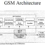
Linux has always started with a kernel distribution, with a set of features ported to a processor. Drivers for common functions, like disk storage, Ethernet, USB, and OpenGL graphics were abstracted enough so they either dropped in or were easily ported. Support for new peripheral devices usually emerged from the community very quickly. Developers grew to love Linux because it gave them, instead of vendors, control.

Freedom comes with a price, however. In the embedded world, where change can be costly and support can be the never-ending story over years and even decades, deploying Linux has not been so easy. Mind you, it sounds easy, until one thing becomes obvious: Linux has been anything but stable when viewed over a period of years. Constant innovation from the community means the source tree is a moving target, often changing hourly. What was built yesterday may not be reproducible today, much less a year from now.

The first attempts at developing embedded Linux involved “freezing” distributions, which produced a stable point configuration. A given kernel release with support for given peripherals could be integrated, built and tested, and put into change control and released. In moderation this worked well, but after about 100 active products showed up in a lab with 100 different frozen build configurations, the scale of juggling became problematic. Without the advantage of being able to retire obsolete configurations, Linux started becoming less attractive for longer lifecycles, and embedded developers were forced to step back and look harder.

In what the folks at The Linux Foundation have termed “the unholy union of innovation and stability”, best brains are trying to bring two efforts – defining what to build and how to build it – to bear to help Linux be a better choice for embedded developers.

LTSI, the Long Term Support Initiative, is backed by many of the companies we discuss regularly here, including Intel, Mentor Graphics, NVIDIA, Qualcomm, and Samsung. LTSI seeks to create a stable tree appropriate for consumer devices living 2 to 3 years, and yet pick up important new innovations in a road-mapped effort. The goal is to “reduce the number of private [Linux] trees current in use in the CE industry, and encourage more collaboration and sharing of development resources.”

The Yocto Project focuses on tools, templates, and methods to build a Linux tree into an embedded distribution. This doesn’t sound like a breakthrough until one considers that almost all embedded development on Linux has been roll-your-own, and as soon as a development team deviates and does something project specific to meet their needs, they lose the benefits of openness because they can’t pull from the community without a big retrace of their steps. The Yocto Project recently announced a compliance program, with Mentor Graphics among the first companies to comply, and Huawei, Intel, Texas Instruments and others participating and moving toward compliance. Yocto has also announced a joint roadmap with LTSI.

With software becoming a larger and larger part of projects – some say 70% and growing – and open source here to stay, these initiatives seek to help Linux be built to last.


The GLOBALFOUNDRIES Files

The GLOBALFOUNDRIES Files
by Daniel Nenni on 09-06-2012 at 9:58 am

There’s a new blogger in town, Kelvin Low from GLOBALFOUNDRIES. Kelvin was a process engineer for Chartered Semiconductor before moving on to product marketing for GF. His latest post talks about the GF 28nm SLP which is worth a read. There was quite the controversy over this Gate-First HKMG implementation of 28nm that IBM/GF/Samsung uses versus the Intel and TSMC Gate-Last implementation. One of the benefits of the GF version being very low power:

SLP targets low-power applications including cellular base band, application processors, portable consumer and wireless connectivity devices. SLP utilizes HKMG and presents a 2x gate density benefit, but is a lower cost technology in terms of the performance elements utilized to boost carrier mobilities.

Anyway, Kelvin is a great addition to GF’s Mojy Chian and Michael Noonan. I look forward to reading more about customer applications at 28nm and beyond.

28nm-SLP technology – The Superior Low Power, GHz Class Mobile Solution
Posted on September 4, 2012
By Kelvin Low
In my previous blog post, I highlighted our collaborative engagement with Adapteva as a key factor in helping them deliver their new 64-core Epiphany-4 microprocessor chip. Today I want to talk about the second key ingredient in enabling their success: the unique features of our

28nm-SLP technology: Enabling Innovation on Leading Edge Technology
Posted on August 30, 2012
By Kelvin Low
It’s always great to see a customer celebrate their product success, especially when it’s developed based on a GLOBALFOUNDRIES technology. Recently, one of our early lead partners, Adapteva, announced sampling of their 28nm 64-core Epiphany-4 microprocessor chip. This chip is designed on our 28nm-SLP technology which offers the ideal balance of low power, GHz class performance and optimum cost point. I will not detail the technical results of the chip but will share a quote by Andreas Olofsson, CEO of Adapteva, in the recent company’s press release…

Innovation in Design Rules Verification Keeps Scaling on Track
Posted on August 28, 2012
By Mojy Chian
There is an interesting dynamic that occurs in the semiconductor industry when we talk about process evolution, roadmaps and generally attempt to peer into the future. First, we routinely scare ourselves by declaring that scaling can’t continue and that Moore’s Law is dead (a declaration that has happened more often than the famously exaggerated rumors of Mark Twain’s death). Then, we unfailingly impress ourselves by coming up with solutions and workarounds to the show-stopping challenge of the day. Indeed, there has been a remarkable and consistent track record of innovation to keep things on track, even when it appears the end is surely upon us…

Breathing New Life into the Foundry-Fabless Business Model
Posted on August 21, 2012
By Mike Noonen
Early last week, GLOBALFOUNDRIES jointly announced with ARM another important milestone in our longstanding collaboration to deliver optimized SoC solutions for ARM® processor designs on GLOBALFOUNDRIES’ leading-edge process technology. We’re extending the agreement to include our 20nm planar offering, next-generation 3D FinFET transistor technology, and ARM’s Mali™ GPUs…

Re-defining Collaboration
Posted on July 18, 2012
By Mojy Chian
The high technology industry is well known for its use – and over-use – of buzzwords and jargon that can easily be rendered meaningless as they get saturated in the marketplace. One could argue ‘collaboration’ is such an example. While the word itself may seem cliché, the reality is that what it stands for has never meant more…


Wireless Application: DSP IP core is dominant

Wireless Application: DSP IP core is dominant
by Eric Esteve on 09-06-2012 at 5:32 am

If we look back in the early 90’s, when the Global System for Mobile Communication (GSM) standard was just an emerging technology, the main innovation was the move from Analog to the Digital Processing of the Signal (DSP), allowing to make unlimited manipulation to an Analog signal, once digitized by the means of a converter (ADC). To run the Digital baseband Processing (see picture), the system designer had to implement the Vocoder, Channel codec, Interleaving, Ciphering, Burst formatting, Demodulator and (Viterbi) Equalizer. Digital Signal Processing science was already heavily used for military application like Radar, but was emerging in telecommunication. The very first GSM mobile handset built based on standard part (ASSP) were using no less than three TI 320C25 DSP, each of them costing several dozen of dollar!

Very quickly, it appears that the chip makers developing IC for mobile handset baseband processing should rely on ASIC technology rather than using ASSP, for two major reasons: cost and power consumption. As one company was dominating the DSP market, Texas Instruments, the mobile handset manufacturers, Ericsson, Nokia and Alcatel had to push TI to propose a DSP core, which could be integrated into an ASIC, developed by the above mentioned OEM. During the years 1995 to early 2000’s, thanks to their dominant position in DSP market, TI was the undisputed leader in manufacturing the baseband processor, through ASIC technology, for the GSM handset OEM, who also developed the IC, at that time.

But a small company named DSP Group, had appeared in the late 90’s, proposing a DSP IP core, not linked to any existing DSP vendor (TI, Motorola or Analog Devices), and even more important, to any ASIC technology vendor. The merge of the IP licensing division of DSP Group and Parthus has been named CEVA and CEVA’ DSP was specially tailored for the wireless handset application. TI competition (VSLI Technology, STMicroelectronics and more) was certainly happy as they could propose an alternative solution to the Nokia et al., but it took some time before these OEM decide to move the S/W installed base from TI DSP to CEVA DSP IP core, that they had to do if they decide to move from TI to another supplier. It was a long route, but CEVA is enjoying today most of the Application Processors chip maker leaders in their customer list, namely:

This help to understand why CEVA has enjoyed 70% market share for DSP IP products in 2011, according with the Linley Group. A 70% market share simply means that CEVA’ DSP IP have been integrated into 1 billion IC shipped in production in 2011! If the Teak DSP IP core was the company flagship in early 2000, the ever increasing need for digital signal processing power associated with 3G and Long Term Evolution (LTE or 4G) has led to propose various new products, the latest being CEVA XC4000 DSP IP core:

And, by the way, the XC4000 target various applications, on top of the wireless handset:

  • Wireless Infrastructure

A scalable solution for Femtocells up to Macrocells

  • Wireless connectivity

A single platform for: Wi-Fi 802.11a/b/g/n/ac, GNSS, Bluetooth and more

  • Universal DTV Demodulator

A programmable solution targeting digital TV demodulation in software
Target standards: DVB-T, DVB-T2, ISDB-T, ATSC, DTMB, etc.

  • SmartGrid

A single platform for: wireless PAN (802.11, 802.15.4, etc.), PLC (Power Line Communication), and Cellular communication (LTE, WCMDA, etc.)

  • Wireless Terminals

Handsets, Smartphones, Tablets, data cards, etc.
Addressing: LTE, LTE-A, WiMAX, HSPA/+, and legacy 2G/3G standards

If we look at the Wireless handset market, it appears that Smartphone and Media tablet, both being based on the same SoC, the Application Processor, will represent the natural evolution, and the analysts forecast the shipment of one billion Smartphone and 200 million Media tablets in 2015. If you look more carefully, you will discover that at least 50%, if not the majority of these devices will be shipped in ASIA, and to be more specific, in China for most of these. An IP vendor neglecting China today would certainly decline in a few years. Looking again at CEVA’s customer list, we can see that many of the Application Processor chip makers selling in these new “Eldorado” markets have selected CEVA. This is a good sign that CEVA will maintain their 70% market share of the DSP IP market in the future!

Like ARM IP core is coming in mind immediately when you consider a CPU core for Application Processor wireless handset phone or smartphone, CEVA DSP IP is the dominant solution for the same. Just a final remark: CEVA is claiming to have design-in their DSP IP in the Chinese version of the Samsung Galaxy S3, which will probably be the most selling smartphone on a world-wide basis…

Eric Esteve from IPNEST


Hardware Intelligence for Low Power

Hardware Intelligence for Low Power
by guruvadhiraj on 09-05-2012 at 9:42 am

Low power is the hottest topic these days. The designers of hardware and software are trying to find instances where they can save power . This article tries to identify the role that can be played by the hardware which traditionally it is always software who drives it.
Continue reading “Hardware Intelligence for Low Power”


Wiring Harness Design

Wiring Harness Design
by Paul McLellan on 09-04-2012 at 5:18 pm

In 2003 Mentor acquired a company doing wiring harness design. Being a semiconductor guy this wasn’t an area I’d had much to do with. But more than most semiconductor people I expect.

But back when I was an undergraduate, I had worked as a programmer for a subsidiary of Philips called Unicam that made a huge range of spectrometers and similar equipment for chemical analysis. These contained a brass cam, hence the name, that moved all the optics that had to be carefully machined. So carefully that the cam cutting lathes were in a temperature controlled room.

Each of these machines also contained a complicated wiring harness to hook up the electronics and the front panel and so on. The production volumes of spectrometers did not justify automating the manufacture of the harnesses. They were assembled by hand by a room full of women seated in front of drawing boards. On each drawing board was a carefully drawn full-scale diagram of the harness with pins to bend the wires around. When a harness was complete, someone would check it, and then the harness would be wrapped with cable-ties and sent off to be put into a spectrometer as it was assembled. The design was clearly done on the drawing boards by draftsmen by hand.

Then when I was at VaST I got involved in many meetings with automotive manufacturers. There is a wiring harness in each car. One of the reasons that automotive was increasingly interested in in-car networks such as CAN bus (unfortunately the C stands for ‘controller’ but ‘car area network’ seemed a better name) was that the wiring harnesses were starting to be embarrassingly large. They might weigh over 50kg, which affected mileage, and they had got so thick it was a real problem to find enough space to thread them through the car to get to the engine compartment, the dashboard, the rear lights and all the other places they needed to go. They were also incredibly complex to design. The wiring in the Airbus 380 caused major delays in the program; I hate to think how complex that wiring must be.

Wally Rhines told me once that the wiring harness products were a surprisingly fast growing business as they got more and more complex. Of course when you are used to putting a few billion wires on a chip, putting together a wiring harness seems almost primitive by comparison. Anyway, I decided to find out more and to watch Mentor’s webinar on the topic. It is given by John Wilson who created the company that Mentor acquired back in 2003.

The webinar is Virtual Design, Testing and Engineering Speeds Electrical and Wire Harness Design. It covers the wiring design process and how it integrates into the system and process designing the vehicle itself. Typically harness design is outsourced to supplier who have to bid on it, then design and manufacture it.


VeSys Design provides an intuitive wiring design tool for the creation of wiring diagrams and the associated service documentation. It has integrated simulation facilities that can validate the design as it’s created, ensuring high quality. VeSys Harness is a tool for harness and formboard design tool with automated part selector and manufacturing report generation. It shrinks the design time and automates many steps in the design process. Vesa is a mid-level product for smaller companies.


For larger problems such as aerospace and automotive with more complex harnesses, there is a more powerful product line called Capital. This is oriented towards enterprise level deployment.

View the webinar here. White papers on electrical and wire harness design are here.


A Brief History of Semiconductors: the Foundry Transition

A Brief History of Semiconductors: the Foundry Transition
by Paul McLellan on 09-04-2012 at 11:30 am

A modern fab can cost as much as $10B dollars. That’s billion with a B. Since it has a lifetime of perhaps 5 years, owning a fab costs around $50 per second and that’s before you buy any silicon or chemicals or design any chips. Obviously anyone owning a fab had better be planning on making and selling a lot of chips if they are going to make any money. A modern fab manufactures over 50,000 dinner-plate sized wafers every month.

In the past, fabs were cheaper. As a result most semiconductor companies owned their own fabs. In fact around 1980 there were no semiconductor companies that didn’t own their own fabs since there would be no way for them to manufacture their designs.

The first thing that happened was that some companies found they had excess capacity in their own fabs because an economically large fab might turn out to be larger than their own needs for their own product lines. Correspondingly, other companies may have the opposite problem: they didn’t build a big enough fab or they were late constructing it, and they could sell more product than they could manufacture.

So semiconductor companies would buy and sell wafers from each other to even out their capacity needs. This was known as foundry business, analogous to a steel foundry. In a similar way, semiconductor companies with shortages would take their designs to other semiconductor companies with surplus capacity (often even competitors) and have them manufactured for them.

The next step in the evolution of the ecosystem was that in the mid-1980s some companies realized that they didn’t need to own a fab to have chips manufactured. These companies would purchase foundry wafers just like any other semiconductor company. These companies came to be called, for obvious reasons, fabless semiconductor companies. Two of the earliest were Chips and Technologies, who made graphics chips for the PCs of the day and Xilinx who made what are now known as field-programmable gate-arrays (FPGAs). They purchased wafers from other semiconductor companies and sold them just as if they’d manufactured them themselves. Chips and Technologies eventually was acquired after falling on hard times, but Xilinx is still the leader in FPGAs today. And despite being number one, it still doesn’t have its own fab, it outsources all manufacturing.

Semiconductor companies with fabs became known as integrated device manufacturers, or IDMs, to distinguish them from the fabless companies. In 1987 the first of another new breed of semiconductor companies was created with the founding of Taiwan Semiconductor Manufacturing Company (TSMC). TSMC was the first foundry, created only to do foundry business for other companies who needed to purchase wafers either because they were fabless or because they were capacity limited. It was also known, when the distinction was important, as a pure-play foundry to distinguish it from IDMs selling excess capacity who would often be competing at the component level with their foundry customers.

Until TSMC and its competitors came into existence, getting a semiconductor company off the ground was difficult and expensive. To build an IDM required an expensive fab. To build a fabless semiconductor company required a complicated negotiation for excess foundry capacity at a friendly IDM which might go away if the IDM switched from surplus to shortage as its business changed. Once TSMC existed, buying wafers was no longer a strategic partnership, you just gave TSMC an order.

This lowered the cost and the risk of creating a semiconductor company and during the 1990s, many fabless semiconductor companies were funded by Silicon Valley venture capitalists. Historically, a semiconductor company had to be large since it had to have enough business to fill its fab. Now a semiconductor company could have just a single product, buy wafers or finished parts from TSMC and sell them.

Over time, another change happened. Many system companies also switched from using the ASIC companies to doing their designs independently and then buying wafers from the foundries. The specialized knowledge about how to design integrated circuits that was lacking in the system companies in the 1980s was gradually acquired and by the 1990s many system companies had very large integrated circuit design teams. The ASIC companies gradually started selling more and more of their own products until they became, in effect, IDMs.

As fabs got more expensive, another change happened. IDMs such as Texas Instruments and AMD that had always had their own fabs found they could no longer afford them. Instead some switched to being completely fabless. For example, AMD sold its fabs to an investment consortium that turned it into a foundry called Global Foundries. Alternatively they kept their own fabs for some of their capacity and purchased additional capacity, typically in the most advanced processes, externally. This was known as fab-lite.

This is the landscape today. There are a few IDMs such as Intel who build almost all of their own chips in their own fabs. There are foundries such as TSMC and Global Foundries who build none of their own chips, they just build wafers for other companies. Then there are fabless semiconductor companies such as Xilinx and Qualcomm along with their fab-lite brethren such as Texas Instruments, who do their own design, sell their own products, but use foundries for all or part of their manufacturing.

A Brief History of Semiconductors
A Brief History of ASICs
A Brief History of Programmable Devices
A Brief History of the Fabless Semiconductor Industry
A Brief History of TSMC
A Brief History of EDA
A Brief History of Semiconductor IP
A Brief History of SoCs


3D Memories

3D Memories
by Paul McLellan on 09-02-2012 at 4:42 pm

At DesignCon earlier this year, Tim Hollis of Micron gave an interesting presentation on 3D memories. For sure the first applications of true 3D chips are going to be stacks of memory die and memory on logic. The gains from high bandwidth access to the memory and the physically closer distance from memory to processor are huge.

Micron have a Hybrid Memory Cube (HMC). Bandwidth to the memory is 128GB/s (1 terabit per second). Each die in the stack is divided up into partitions, each of which is a 2-bank autonomous memory element. In turn, these are grouped in the vertical direction into “vaults” that consist of the same partition on each die all linked up together using through-silicon-vias (TSVs). In turn, the memory die are stacked on top of a single logic die to form the whole cube, with fully integrated DRAM and logic.

This way of dividing up the cube is also used to divide up the simulation. Initially partition level simulations are used to capture general noise to timing sensitivity. Multi-partition simulations (same die) capture inter-partition noise coupling, and vault level (vertical slice) capture die to die noise coupling. Finally, cube level simulations capture the impact of system power delivery network (PDN), resonance etc. The fact that there is so much repeated in the architecture make this very hierarchical approach viable.

At the partition level, simulation focused on power-grid impedance analysis, voltage drop analysis, full spice-level simulation with the power grid and decoupling all modeled. Apache’s Totem static analysis was used to correct layout and to validate that the silicon and the model matched.


At the vault level (multi die) Apache’s chip-power-model (CPM) was used to create dummy layers and the simulation focused on ensuring that layers were adequately isolated from noise. Then at the level of the system PDN the focus was on noise and resonance and adequacy of decoupling.

Takeaways from modeling the hybrid memory cube:

  • complexity is a function of how tightly coupled different parts of the system are and how much concurrent activity is allowed
  • physically partitioning the device simplifies design, modeling and simulation
  • 3D challenges must be overcome in parallel.

The Micron presentation is here in Apache’s CPS microsite.


A Brief History of Cadence Design Systems

A Brief History of Cadence Design Systems
by Daniel Nenni on 09-01-2012 at 8:10 pm

EDA software for IC and system design became a commercial business in the early 1980s. In those days, 3 companies – Daisy Systems, Mentor Graphics, and Valid Logic Systems – dominated the emerging EDA industry. However, two small startups that emerged in the early 1980s grew rapidly and merged to form Cadence Design Systems in 1988.


One of those startups was ECAD, which was founded by Glen Antle and Paul Hwang in 1982. Unlike the leading EDA vendors, who also sold workstations, ECAD provided only software. The company developed and sold Dracula, an IC layout verification product that came into widespread industry use.

The other startup, SDA Systems, was founded in 1983 by Jim Solomon, a former product manager at National Semiconductor. Also a software-only company, SDA offered IC physical design tools within an integrated “framework” that could also accommodate third-party tools. Joe Costello, a former R&D manager at National Semiconductor, joined SDA Systems in 1984 and became its president in 1987.

In Feb. 1988 ECAD bought SDA for $72 million in a stock swap. A new company, Cadence Design Systems, was incorporated June 1, with Costello as president and CEO. Within a year Cadence had become the leading provider of IC design automation tools. Under Costello’s charismatic leadership over the next 9 years, Cadence completed a number of strategic acquisitions, built widely-used product lines, moved into system-level and PCB design, and made design services a key part of its strategy.

1989 was a formative year in several respects. First, Cadence bought Gateway Design Automation, developer of the Verilog hardware description language. (A year later Cadence put Verilog into the public domain, and it became the most widely used hardware description language). Secondly, Jim Solomon started the Cadence Analog Division, launching an effort in which Cadence became the undisputed leader in custom/analog design automation tools. Third, the purchase of Tangent Systems boosted Cadence’s leadership in IC layout automation.

Here are some key Cadence milestones since 1989:
· 1991 – Acquired Valid Logic Systems and became the EDA revenue leader.
· 1993 – Bought Comdisco Systems, a pioneer of system-level design.
· 1994 – Launched Spectrum Services consulting group.
· 1997 – Acquired HLD Systems (design planning) and Cooper & Chyan Technologies (automatic routing). Jack Harding, Cooper & Chyan CEO, became Cadence CEO.
· 1999 – Harding succeeded by Ray Bingham as CEO. Cadence acquired OrCAD (PCB design) and Quickturn (emulation).
· 2001 – Avanti found guilty of stealing Cadence trade secrets, ordered to pay $194 million restitution.
· 2002 – Cadence Genesis design database offered to EDA industry as “OpenAccess.” Cadence bought Simplex Solutions (IC physical verification).
· 2004 – Mike Fister became president and CEO.
· 2005 – Cadence acquired Verisity, pioneer of coverage-driven verification.
· 2008 – Lip-Bu Tan became president and CEO.
· 2010 – Cadence EDA360 vision proposed expanded role for EDA. Purchase of Denali Software strengthened Cadence position in design and verification IP.

Fast forward to 2012, and Cadence has enjoyed three years of steady growth in revenues and earnings. 30 years after the launch of ECAD, Cadence employs approximately 4,900 people worldwide, reported 2011 revenues of $1.1 billion, and provides a wide range of IC, PCB and system design products that are used by nearly every semiconductor and electronic systems provider today.

A special thanks to Richard Goering, Senior Manager, Technical Communications, at Cadence, for compiling this data. Richard has covered EDA since 1985 most notably as EE Times’ EDA editor for 17 years, where he wrote hundreds of articles for both the print and on-line editions of the electronics industry’s premier weekly newspaper.

A Brief History of Semiconductors


The Need for OASIS in Post-layout IC Databases

The Need for OASIS in Post-layout IC Databases
by Daniel Payne on 08-31-2012 at 7:20 pm

OASIS is a hierarchical IC file format used for IC designs that is gradually replacing GDS II throughout the mask data stages. The compelling reason for using OASIS has always been the reduction of file size, and speed up of processing times through the use of hierarchy and fewer translation steps.

At the 45nm node an actual M1 layer from design had a file size of 0.066 Gb, however after going through pre-OPC, post-OPC and Fracture stages that same M1 layer has ballooned in file size to 59 Gb, according to a White Paper authored by four Mentor specialists (Deployment of OASIS in the Semiconductor Industry – Status, Dependencies and Outlook). The following figure shows in blue how this file size expansion happens at each stage:


File size and hierarchical content across the 4 different stages of mask data processing for a real 45nm M1 example. The “hierarchy” data is computed as the number of flat geometries divided by the number of hierarchical geometries. These results show that the post-OPC step has the highest return from an investment in hierarchical compression technology such as the OASIS format.

EDA companies rapidly adopted OASIS as a file format however it took a few years longer for the Fracture data stage to use OASIS based on survey results:


Survey results showing OASIS adoption by technology node, broken down by the data-prep handoffs. These results indicate that OASIS has been adopted by a significant fraction of companies doingOPC as early as 65nm, but that hand-off of fractured data in OASIS has lagged by as much as 2 processnodes.

Just how much compression should you expect when changing from GDS II to OASIS? The average compression is 18.57 at the design stage, and 14.24 at the post-OPC stage:


Data size savings of OASIS vs GDSII, as measured by compression ratio of the file sizes, fordesign and post-OPC layout files. Although the median compression ratios are very similar, the entiredistribution of compression rations for post-OPC files consistently shows smaller values (shifted to theleft) than the distribution for design files.

One factor that slowed adoption of OASIS from GDS II has been the low costs combined with expanding capacity of disk storage.

Summary
Work to define OASIS started back in 2001, became a SEMI standard in 2005, and was quickly adopted by EDA vendors. The post tape-out vendors are using OASIS in Pre-OPC, Post-OPC and Fracture stages to reduce runtimes by 3X and reduce file storage sizes by 3X. Old file standards like GDS II have given way to OASIS gradually over the past decade.