Bronco Webinar 800x100 1

Chip Aware System Design

Chip Aware System Design
by Paul McLellan on 09-24-2012 at 5:45 pm

On Wednesday this week Ansys/Ansoft/Apache are presenting a new webinar Chip Aware System Design. It is presented by Dr Steven Gary Pytel Jr of the Ansoft part of Ansys, and Matt Elmore of the Apache subsidiary. The topics that will be covered include:

  • Power Delivery Network (PDN) design requirements
  • ABCD Matrix theory
  • SYZ Matrix theory
  • Chip-level Extraction
  • Effect of Chip inclusion on time and frequency domain system simulations

The webinar is in two parts, the first part fairly theoretical and mathematical (as you can see from the above list), that gives the foundation for analysis, especially frequency domain analysis. The second part takes that theory and uses it for practical analysis of power delivery networks.

The goal is that by the end of the webinar, attendees will be able to:

  • gave a basic understanding of impedance, transmission and scattering parameters
  • perform basic analyses on return and insertion loss
  • understand the impact of chip parasitics in both time and frequency domains
  • create and analyze “what if” test cases for real chip, package and PCB designs


The webinar is at 11am Pacific Time on Wednesday, 1pm on the east coast and corresponding times elsewhere. Pre-registration is here.


SAME 2012 Conference on October 2-3 in Sophia is coming soon!

SAME 2012 Conference on October 2-3 in Sophia is coming soon!
by Eric Esteve on 09-24-2012 at 11:01 am

This is the 15[SUP]th[/SUP] anniversary for the SAME Conference, dedicated to innovation on Microelectronics. Sophia-Antipolis is not only close to Mediterranean sea, but also at the heart of Telecom valley in south of France, with Texas Instruments design center dedicated to Application Processor design (OMAP), Cadence research center (managed by Jacques-Olivier Piednoir) developing Virtuoso Full custom layout edition tools (along with other team in India and the US), ST-Ericsson and many more. This area is a nice place to attract high level engineers, this explains why many companies, including ARM, Cambridge Silicon Radio (CSR), Intel, NVIDIA, Maxim, Mentor Graphics and Synopsys have a subsidiary here. To see the full company list, just go here. If you want to register, click on the SAME Logo:

I plan to attend the conference, especially the morning session about MIPI, a Tutorials given by Texas Instruments (M-PHY), Arteris (LLI Implementation challenges) and Cadence (New MIPI protocols), but, if you’re more interested about RF Modeling and RF Design, the session run in parallel. The conference agenda can be found here, just click on the agenda:

Also, you should not miss the Keynote talk from Mike Muller, ARM CTO, “A 2020 View & Perspective”:
Comparing the original ARM design of 1985 to those of today’s latest microprocessors, Mike will look at how far has design come and what EDA has contributed to enabling these advances in systems, hardware, operating systems, and applications and how business models have evolved over 25 years. He will then speculate on the needs for scaling designs into solutions for 2020 from tiny embedded sensors through to cloud based servers which together enable the internet of things. He will look at what are the major challenges that need to be addressed to design and manufacture these systems and proposes some solutions.
Mike Muller was one of the founders of ARM. Before joining the Company, he was responsible for hardware strategy and the development of portable products at Acorn Computers and was part of the original ARM design team. He was previously at Orbis Computers who developed network computers. At ARM he was VP, Marketing from 1992 to 1996 and EVP, Business Development until October 2000 when he was appointed Chief Technology Officer. In October 2001, he was appointed to the board of ARM Holdings plc.

If you plan to attend it will be a pleasure to meet you there!

By Eric Esteve from IPnest


A Brief History of Helic

A Brief History of Helic
by Daniel Nenni on 09-24-2012 at 10:00 am

As I have mentioned before, you can tell al lot about a company by their CEO. The previous trip I made to Taiwan was with Helic co-founder and CEO Dr. Yorgos Koutsoyannopoulos. One of the benefits of my job is I get to spend time with some very interesting people from around the world and this was no exception.

Prior to founding Helic, Yorgos worked as a research engineer of ICCS (an academic institute in Athens), in technology development projects for European corporations such as ST Microelectronics, Atmel-ES2 and Infineon. He received his Ph.D. and Diploma in Electrical Engineering from the National Technical University of Athens and he has attended executive courses on leadership and marketing at LBS and Harvard. Yorgos is a well-rounded guy and very personable, and a pleasure to work with.

Helic is an EDA specialist developing innovative and disruptive design automation technologies for the semiconductor market. Founded in May 2000, the company is backed by strategic and venture capital investors including the legendary Andy Bechtolsheim, Synopsys (formerly Magma), and Fujitsu. Helic reaches its customers with a business model combining EDA tools, IP and services, with a mission to enable first-pass silicon while greatly shortening the development cycles of high-speed digital, analog RF and millimeter-wave ICs.

Helic has more than 60 corporate customers and more than 1,500 users who design chips for a wide range of applications; from cellphone standards (1-2.1GHz), Bluetooth and WiFi (2.4-5.8GHz) to Gbit Ethernet, to multi-core CPUs and GPUs and to mm-wave applications. Helic is also the only emerging EDA company that I know of that has a full silicon correlation lab to perform on-chip measurements up to 70GHz.

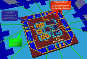
Helic’s background technology is a unique high-speed parasitics extraction methodology. It was conceived to address a critical missing link in custom IC design flows and accelerate the development of complex RFICs and systems-in-package by enabling rapid, whole-chip electromagnetic modeling early in the design flow. The technology has been in use since 2000 by fabless companies and silicon IDMs worldwide.

Helic develops and provides EDA technology that enables rapid electromagnetic synthesis and modeling of on-chip passive devices, high-frequency interconnects, bondwires and package parasitics. At the core of Helic’s technology, an ultra-fast RLCK modeling engine offers signoff accuracy comparable to full-wave EM simulators, while outperforming the fastest reported EM engines by 100x or more in terms of speed and capacity. Helic has made significant advances in the development of efficient design flows that help designers overcome some known obstacles in the development of high-performance RF and high-frequency ICs.

Helic’s tool flows help fabless semiconductor and IDM customers achieve:

  • Minimization of silicon real estate employed by on-chip inductors and passives.
  • Centering of challenging high-speed circuits such as wideband amplifiers and oscillators.
  • Rapid simulation of signal integrity aspects such as inductance- and package-loaded transient response.
  • Concurrent low-noise/low-power RF circuit optimization, based on the synthesis of passive devices.
  • Model higher-order effects on power grids and clock networks due to magnetic coupling.

The company has 50 highly skilled professionals in its ranks today (30% hold a PhD, 35% a Master’s Degree, and another 30% a Bachelor); offices in San Francisco and San Jose, CA, Athens, Greece, and Yokohama, Japan and a sales network of partners in Korea, Taiwan, Israel, and China.

At this year’s Design Automation Conference in San Francisco, Helic and TSMC co-organized a workshop on “CMOS Design at 60 GHz and Beyond: Capabilities and Challenges”, with speakers from Silicon Image, TSMC, Helic, KU Leuven, Integrand Software, and Presto Engineering. A white paper on the workshop can be found HERE.


Taiwan Travel Explained!

Taiwan Travel Explained!
by Daniel Nenni on 09-23-2012 at 7:00 pm

Whenever people hear that I travel internationally one week a month they cringe at the thought of crowded airports, 12 hour flights, jet lag, and days packed with meetings. I generally shrug, accept the label of travel warrior, and say it is all part of doing business in the semiconductor ecosystem. But in reality, it is not as bad as it sounds, especially if you include the knowledge gained as part of the ROI calculation.

First and foremost, I rarely travel alone. As a business consultant I work for the CEOs of emerging technology companies advising them on a variety of topics. I wish I could say they learn more from me than I do from them but that is rarely the case. Successful emerging technology CEOs are a unique breed and are almost always a pleasure to work with. These CEOs wear so many hats and work so many hours that I get a headache just thinking about it. Every trip brings new problems and new ways to solve them which is an excellent learning experience on many different levels.

As a frequent traveler, I get perks from airlines and hotels fit more for a king than a regular working person. Executive lounges at airports are a good example. Right now I’m in the EVA airlines Evergreen Lounge sipping champagne and eating rice crispy treats (I don’t like caviar). Seat upgrades, personalized in-flight service, priority baggage handling etc…, it really does take the sting out of air travel. Even the airport garage I park my car in has frequent parking perks: Car washes, oil changes, priority shuttle services etc…

The hotels are the most generous. I get corporate rates for the cheapest rooms and the upgrades just keep coming. The rooms I usually get are huge with every modern convenience you can imagine. Sometimes the bathrooms are absolutely amazing. As you approach the toilet the seat raises, auto flushes, washes and dries, and closes as you walk away, semiconductor technology at its finest! The hotel welcome baskets are quite tasty and quite fattening, so I always bring my gym clothes to burn the extra calories that come with travel. Exercise also helps with jet lag. Another way I avoid jet lag is to NOT eat airline food and drink lots of water, believe it.

The boxes in the picture are Taiwan tea which is an interesting story in itself. A fellow international traveler convinced me that green tea is the key to a long and fruitful life and I have been drinking it ever since. That was more than ten years ago and I still believe it. I started with Japanese green tea but now Taiwan tea is my favorite.


In the hills right above the TSMC fabs in Hsinchu Science Park is one of the more famous green tea farms which I visit quite frequently. As the Taiwanese tea legend goes:

A tea farmer’s crop was infested by little green-leaf worms. Trying to recover from this catastrophic loss, the tea farmer went into town to sell his low-grade tea anyway. As it turns out the tea had a unique flavor and gained huge popularity. This guy was a great salesman for sure! When the tea farmer returned to his village and told the story it was viewed as bragging so they called his tea “puffing tea”, puffing means bragging in Taiwanese. The legend also says that Puffing Tea was a favorite of Britain’s Queen Victoria (1800’s) and she gave it the name Oriental Beauty Tea. European aristocrats later named it Champion Oolong Tea.

The tea is harvested three times a year. In the spring it is green tea (the green box) which has a mild flavor. Next harvest is orange tea. Fall harvest is red tea with the strongest flavor. If you look on the top of the boxes there are pictures of green-leaf worms which determines the price. The more worms the higher the price. There is more on Taiwan Tea Farms HERE. Even though Starbucks has invaded every corner of Taiwan, tea is still a big part of modern life here.


Cadence Mixed Signal Technology Summit

Cadence Mixed Signal Technology Summit
by Paul McLellan on 09-21-2012 at 6:46 pm

Yesterday I attended some of the Cadence mixed-signal technology summit. The day ended with a panel session on Are We Closing the Gap Yet in Mixed-signal Design? Richard Goering moderated. The panelists were all mixed signal experts:

  • Nayaz Khan of Maxim
  • Nishant Shah of Broadcom
  • Shiv Sikand of IC Manage
  • Bill Meier of Texas Instruments
  • Bob Chizmadia of Cadence

The panelists were invited to say which gaps have been closed and where the current gaps are. There seems to be a large amount of agreement, in fact, in both the panel session and some of the sessions earlier in the day.

Problem #1: Adding analog into the digital flow is a sort of second class citizen, especially when trying to use SystemVerilog. Especially Connect Modules. And never mind multi-language.

Problem #2: People need to know a lot. Finding individuals who can work with object-oriented code and understand analog and understand power is really hard. As a result, AMS designs require an extra level of support. TI even have a program called AMSmadeEZ the Bill heads up. Ideally you want a separate team for AMS verification since it is much more effective if people do it a lot and not just a couple of times per year. TI and Maxim seemed to do this.

Problem #3: It is really hard to keep all the files aligned between the analog world and the digital world. Especially keeping the models the digital people need of the analog aligned with the analog development itself. Hierarchy doesn’t always match. Wires can only carry voltage or current but not both, further complicating things. AMS assertions don’t work the same in all the different simulators.

Problem #4: When using CPF (for power policy) in the digital world it works well. But the checks with analog are not clean. There is no way to ensure that when a domain is powered down that an analog gate doesn’t float, for example. Or if the analog already contains a level shifter to make sure it doesn’t get doubled.

Problem #5: At 20/22nm and 14nm the problems are daunting. The process, tools and methodology are all developed concurrently. The number of design rules explodes. Variability goes way up.

On the other hand there have been huge advances in the last 5 years. Back when I was at Cadence we kicked off a program called Superchip that was supposed to merge the analog and digital design environments and also move them onto OpenAccess. It rapidly became clear we were years away from being able to do that (despite sales having committed it to a huge customer who had better remain nameless). But a lot of that vision is now a reality.


Atrenta Wins Gold

Atrenta Wins Gold
by Paul McLellan on 09-21-2012 at 6:16 pm

What is the most read article on design on EE Times website? Brian Bailey has an article up running through the top 10. It turns out that the #1 article is Understanding Clock Domain Issues by Saurabh Verma and Ashima S. Dabare of Atrenta. It actually had more than double the views of the second place paper. Checking clock domain crossing is complicated but really important. I’ve been suprised at how many views blogs get here when I write about it.

But wait, there’s more. Atrenta also had a second article in the top 10. Coming in at #9 is Power Awareness in RTL Design Analysis by Narayana Koduri.

But wait, there’s even more. John Cooley does a survey of users at DAC. The #1 hot tool at DAC was SpyGlass Power. Well, it was actually first equal, sharing the spot with Calypto’s PowerPro RTL and Apache’s PowerArtist. Clearly power reduction is a hot(!) topic.

For the silver medal, in Cooley’s #2 place, was Atrenta IP Kit (sharing with IC Manage’s IP Central and Sonics SGN). Design really is changing towards much more of an IP assembly process and ensuring the quality of the IP and managing all the views is really important.


The End of an Era

The End of an Era
by Paul McLellan on 09-21-2012 at 5:45 pm

I drove down from San Francisco, where I live, to Silicon Valley this morning. Something odd was going on. As I approached San Francisco Airport there were a couple of buildings with lots of people standing on the roof. As I got further south, the bridges over the freeway all had lots of people just milling around. It was when I got to Moffat and the crowds were huge that I remembered that the space shuttle was passing through the bay area on its way to its final home in Southern California.

I was actually in a conference room when the shuttle flew by, but somehow we managed to miss it even though we were supposedly facing in the right direction. But John Linthacum, a Cadence AE, didn’t. He got the picture above (click for a larger version).

Who knows whether there will ever be manned space program again in our lifetimes? As the capability of computers improves and technology like driverless cars becomes mainstream, the advantages of manned versus automated exploration get less and less. Of course a lot of the improved technology comes about as a result of improvements in semiconductor manufacturing and in EDA that drives it (obligatory semi reference to justify blogging on SemiWiki).

It is a fun coincidence that the Mars rover Curiosity should have just landed there at roughly the same time as the Space Shuttle finally goes to its retirement home. When I heard about the process by which it landed, with a mother ship and the strongest parachute ever built and a sort of flying saucer lowering the rover onto the surface it seemed unlikely to work. Remember it is minutes away for any radio signal so it is a completely automated landing sequence. Mars was so far away that it took 14 minutes for the Jet Propulsion Laboratory (JPL) to even know it had landed successfully, touching down at a vertical speed of about 2 feet per second.

But for sure it feels like the end of an era…


Displaced but Looking to Add EDA Tools Skills?

Displaced but Looking to Add EDA Tools Skills?
by Daniel Payne on 09-21-2012 at 1:12 pm

In this tough economy you may find yourself displaced and looking for the next opportunity. If you’d like to add some new EDA tool skills, then check out what EMA Design Automation is offering with free Cadence OrCAD training. Continue reading “Displaced but Looking to Add EDA Tools Skills?”


Virtual Prototype your SoC including Arteris FlexNoC and optimize architecture using CPAK from Carbon

Virtual Prototype your SoC including Arteris FlexNoC and optimize architecture using CPAK from Carbon
by Eric Esteve on 09-21-2012 at 7:37 am

I have talked about Virtual Prototyping a SoC including FlexNoC Network on Chip IP from Arteris by using Carbon Design Systems set of tools in a previous post. A blog, posted on Carbon’ web, is clearly explaining the process to follow to optimize a fabric (FlexNoC) successively using the different tools from Carbon. Bill Neifert, CTO with Carbon Design Systems introduces the SoC context: “Fabric optimization is a prime area for architectural analysis. SoCDesigner Plus is an ideal tool for this and since it’s the only virtual prototype tool which will deliver 100% accurate results it’s extremely valuable for making crucial design decisions. It also made a lot of sense as well that Arteris IP would be requested. Their constant stream of press releases with customer design wins is pretty strong evidence of how widely their IP has been adopted.”

The first step is to create a 100% cycle accurate models of Arteris FlexNoC interconnect models by using Carbon Model Studio. To do so, Eric Sondhi from Carbon has used the FlexNoC project file (.PDD file) that matched AXI interconnect configuration and initial memory map definition of the system, this project file being generated either by Arteris, or by the designer using Arteris’ tools. Then, entering the project file into the FlexNoC tool to generate the Verilog RTL for the specific FlexNoC, lead to the 100% cycle accurate description. As Eric Sondhi point it out, the value that 100% cycle accurate models provide by enabling SoC developers to guarantee their functional behavior and performance results will match final silicon is huge!

Screenshot of the Arteris FlexNoC CPAK

At this stage, the SoC designer can start virtual prototype the design, providing he has already created (or re-use) the various models describing the different functions, also generated by Carbon Model Studio. Virtual prototyping is done by assembling the different models together, with SoCDesigner Plus tool from Carbon. Once this task has been completed (there is a very accurate description of this process in Eric’s blog), the designer can start “to have fun”, and move to the Carbon Performance Analysis Kits (CPAK) tools.

A9 Read Latencies from FlexNoC Input

This last step is precisely described by Eric on a real-world ARM Cortex A9 based system with DMA-like traffic generators running Carbon’s ARM boot & initialization code with Performance Validation software provided in some of other CPAKS from carbon. For SoC architect, this should be the most amazing task, where he runs SoC performance analysis simulations and observe latency on both sides of the FlexNoc, then try various options in order to optimize architecture.

Read Latencies from FlexNoC Output

At this stage, you should go and read Eric’s blog to more precisely all the possibilities offered by the joint Carbon/Arteris solution, as it offers design teams a way to easily create and import accurate Arteris FlexNoC interconnect models for Carbon SoCDesigner Plus: the new Carbon/Arteris flow allows Carbon’s SoCDesigner Plus users to use Arteris FlexNoC to configure their NoC interconnect fabric IP and then upload the configuration to Carbon IP Exchange. The web portal then creates a 100% accurate virtual model of the configuration and makes it available for download and use in SoCDesigner Plus. “We see strong demand for models of Arteris’ NoC interconnect IP,” states Bill Neifert, chief technology officer at Carbon Design Systems®, the leading supplier of virtual platform and secure model solutions. “Our partnership with Arteris enables engineers to make architectural decisions and design tradeoffs based upon a 100%-accurate virtual representation.”

By Eric Esteve from IPNEST


Over-under: Apple, 52M iPhones in 4Q

Over-under: Apple, 52M iPhones in 4Q
by Don Dingee on 09-20-2012 at 8:15 pm

I’m in a Twitter conversation with some friends, with the subject: how many phones can Apple ship in the 4th quarter?

A respected analyst said 52M is “an easy mark” for Apple; others are saying 58M is the target for just the iPhone 5 in 4Q. However, the start for the iPhone 5 has been anything but easy. Oh, the orders are probably there – 2M iPhone 5 orders in 24 hours indicates really strong demand.

It’s been a good year. Apple’s 1Q iPhone shipments were 35M units, 2Q were 26M units, and we’re obviously waiting on a figure for 3Q.

The questions for 4Q are two-fold, however. One is supply, the other is demand.

Apple’s supply problem is pointing to their selection of a Sharp 4″ LCD display, at least for the initial build. Rumors have it the yield at Sharp is less than 40%. Other sources are LG and Japan Display, but no word on how well they will ramp up. Sources say capacity of each supplier is something like 7M units per month, if everything goes right. There are also unspoken concerns about the A6 chip inside, but my guess is Samsung has that pretty well in hand. Since the display and memory have been taken away for the iPhone 5, Samsung doesn’t want to be the long pole in the tent on the A6.

Then there’s demand. Apple is now saying they are 3 to 4 weeks from filling the initial orders. I’d also question how prior demand for iPhone 4S units will hold up in the face of iPhone 5 availability. Both those factors may slow down the frenzied pace of orders just a bit. One thing that might help would be if Lucy Koh somehow puts the kibosh on shipments of the Samsung Galaxy SIII. There’s also the remote possibility that the Nokia Lumia 920 and the just announced HTC 8x will ship as expected in time for the holidays, Microsoft willing, and might actually take some demand.

The numbers being tossed around for Apple are huge, to the point where one has to question if they can ship as many orders as they can book. I have no doubt this gets worked out in 2013, but the pressure is on and I think 4Q12 is in some doubt.

I say “under” 52M, with new, untested suppliers in the critical path. Discuss.