RVN! 26 Banner revised (800 x 100 px) (600 x 100 px)

MemCon 2012: Cadence and Denali

MemCon 2012: Cadence and Denali
by Eric Esteve on 08-20-2012 at 7:00 am

I was very happy to see that Cadence has decided to hold MEMCON again in 2012, in Santa Clara on September 18[SUP]th[/SUP] . The session will start with “New Memory Technologies and Disruptions in the Ecosystem”from Martin Lund.

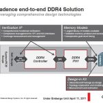
Martin is the recently (March this year) appointed Senior VP for the SoC Realization Group at cadence: he is managing the group in charge of IP, including the Memory Controller product line (DDRn, LPDDRn or WideIO) and PCI Express IP that Cadence has inherited after Denali acquisition. With these products, Cadence is competing head-on with Synopsys and, even if the revenue generated by DDRn IP license is kept confidential by Cadence, my guess is that both companies are very close in term of market share.

The charter of Martin Lund is crystal clear: capitalize on Denali acquisition and the related IP product lines, leverage on know how (SerDes development, Ethernet Controller and more) acquired by Cadence when doing design service for they demanding customers, to build a real IP business unit, capable of competing head to head with Synopsys. I have no doubt that Cadence has the right designers, marketers and the IP products “backbone” to turn this strategy into success. Then, it will be a question of realization, as usual, and maybe this strategy should be comforted by some cleaver acquisition to grow the business faster. We will see in the future…

If you want to register, just go here.

If you prefer to have a look at the conference agenda first, then you can click here… or read this blog, I will tell you why I think going to MemCon 2012 is a good idea!

The first time I attended to MemCon was in 2005, at that time I was representing PLDA and I came with a Xilinx based board with our x8 PCI Express IP core integrated (this was the first X8 PCIe IP running on FPGA worldwide, and yes, thanks, we sold a lot of boards, as well as a lot of PCIe IP to our ASIC customers). I must say I was very impressed by MemCon, as I had the chance to listen to a few presentations.

All these presentations, whether about PCI Express or more specifically about Memories, had in common to be very deep technically, and very informative. It was not pure marketing, the audience would really learn about the topic (I remember a presentation about PCI Express protocol given by Rambus – I was PCIe Product Marketing Director- and I learned more than during the long discussions I had with our designers).

The second reason why I was impressed was when I realize that Denali could manage such high quality event. At that time, in 2005, Denali revenue was probably in the $30M to $40M –or less, they never share it. That’s a good size when you run IP and VIP business, but you have to compare it with the companies presenting at MemCon: Rambus was the smallest, the others being Micron, Samsung and the like. Denali has been bought in 2010 for $315M by Cadence (or seven time their 2009 revenue!), and this was not by chance. The best Denali strength was their marketing presence. Everybody knows about the Denali Party during DAC, and about Memcon. So everybody knows about Denali in the SC industry. Can you think about that many company of that size able to create such a level of awareness? Denali was really the benchmark in term of marketing in the CAE, IP or VIP industry! Now, you better understand why they could have been sold for 7X their yearly revenue…

To come back to the conference, here is a short list of the presentations (you will find more here):

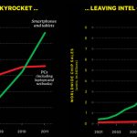
  • Navigating the Post-PC Worldfrom Samsung
  • Simplifying System Design with MRAM—the Fastest, Non-Volatile Memoryby Everspin
  • Paradigm Shifts Offer New Techniques for Analysis, Validation, and Debug of High Speed DDR Memoryfrom Agilent
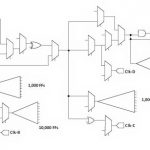
  • LPDDR3 and Wide-IO DRAM: Interface Changes that Give PC-Like Memory Performance to Mobile Devicesby Marc Greenberg from Cadence

Just a word about the last one from Marc Greenberg: I saw his presentation in Munich, during CDN Live in May, I can tell you that this guy knows very well the topic. Don’t hesitate to ask him questions (like I did), you will get answer, and you could even start a longer and informative discussion after the presentation (like I did too!).

I don’t know if I could make it and go to MemCon (Santa Clara is a bit far from Marseille), but you should do it, and tell me if I was wrong to send you there.

By Eric Esteve from IPNEST


A Brief History of SoCs

A Brief History of SoCs
by Daniel Nenni on 08-19-2012 at 10:00 am

Interesting to note; our cell phones today have more computing power than NASA had for the first landing on the moon. The insides of these mobile devices that we can’t live without are not like personal computers or even laptops with a traditional CPU (central processing unit) and a dozen other support chips. The brain, heart, and soul of today’s cell phone is a single chip called an SoC or System on Chip, which is a literal definition.


Sources: Device Sales: Gartner, IDC; Chip Sales: ARM, Wired Research

The demands on cell phones are daunting. What were once simple tasks; talk, text, email, now include photos, music, streaming video, GPS, and artificial intelligence (Apple Siri / Android Robin), all now done simultaneously.

I worked my way through college as a field engineer for Data General mini computers. CPUs were dozens of chips on multiple printed circuit boards, memory was on multiple boards, I/O was a board or two. Repairing computers back then was a game of board swap based on which little red lights blinked or stopped blinking on the front panel. My first personal computer was a bit more compact. It had a mother board with multiple chips and slots to plug in other boards for video, disk, modem, and other interfaces to the outside world. Those boards are now chips on a single mother board which is what you will see inside your laptop.

Today, this entire system is on one chip. Per Wikipedia:

A system on a chip or system on chip (SoC or SOC) is an integrated circuit (IC) that integrates all components of a computer or other electronic system into a single chip. It may contain digital, analog, mixed-signal, and often radio-frequency functions—all on a single chip substrate.

Let’s look at the first iPhone tear down which can be found HERE. The original iPhone was released June 29, 2007 and featured:

  • 480×320 display
  • 16GB storage
  • 620MHZ single core CPU
  • 103MHZ GPU
  • 128MB DRAM
  • 2M pixel camera

Compare this to the current iPhone4s tear down which can be found HERE. The iPhone 4s was released October 4, 2011 and features:

  • 960×640 display
  • 64GB storage
  • 1GHZ dual core CPU
  • 200MHZ GPU
  • 512MB DRAM
  • 8M pixel camera

There is a nice series of Smart Mobile articles on SemiWiki which cover the current SoCs driving our phones and tablets:

It will be interesting to see what the iPhone5 brings us but you can bet it will be an even higher level of SoC integration; a quad core processor, a 2048×1536 display, and a 12M pixel camera, yet in a slimmer package.

The technological benefits of SOCs are self-evident: everything required to run a mobile device is on a single chip that can be manufactured at high volumes for a few dollars each. The industry implications of SoCs are also self-evident: as more functions are consolidated into one SoC semiconductor companies will also be consolidated.

The other trend is the transformation from traditional semiconductor companies (IDMs and fabless) to semiconductor intellectual property companies such as ARM, CEVA, and Tensilica. This is partly due to the lack of venture funding made available to semiconductor start-ups (it costs $100M+ to get a leading edge SoC into production), but also due to the mobile market which demands SoCs be highly integrated and power efficient with a very short product life. As a result, hundreds of semiconductor IP companies are emerging and hoping to ride the SoC tidal wave leaving traditional semiconductor companies in the wake.

A Brief History of Semiconductors

A Brief History of ASICs
A Brief History of Programmable Devices
A Brief History of the Fabless Semiconductor Industry
A Brief History of TSMC
A Brief History of EDA
A Brief History of Semiconductor IP
A Brief History of SoCs


Ex ante: disclose IP before, not after standardization

Ex ante: disclose IP before, not after standardization
by Don Dingee on 08-17-2012 at 3:46 pm

Many of the audience here are involved in standards bodies and specification development, so the news from the Apple v. Samsung on the invocation of ex ante in today’s testimony is useful.

I worked with VITA, the folks behind the VME family of board-level embedded technology, on their ex ante policy several years ago, and can share that insight. I’m not a lawyer, nor do I play one on TV, so this is the highly simplified, non-legalese version of the rules. Consult your legal department with any questions.

  • If you’re working on a specification with a standards body, and it looks like your company has IP in the form of a patent or patent pending applies, you must disclose that. You’re not yielding your IP rights when doing so, and in fact you’re protecting them for later.
  • If the standards body and its membership decide that the technology is appropriate for use in the specification, it’ll proceed through the normal channels of approval with the accompanying IP disclosures so balloters are aware of the possible implications.
  • The standards body and its membership might decide to re-engineer the specification to avoid impinging on the IP in question.
  • Should the standard be approved with the IP in question, there will be a discussion of FRAND – fair, reasonable, and non-discriminatory licensing for use of the IP inside.

What this prevents is the unwitting or unvigilant members of a standards body picking up a duly approved specification, implementing it, then finding themselves the target of an IP claim from the company that got their IP engineered in.


ETSI, the European telecom folks behind 3GPP, LTE and other specifications, just whacked Samsung over the head with their ex ante policy in testimony today. Three articles for more reading.

CNET: Former ETSI board chief: Samsung flubbed disclosures
EETimes: Apple Claims Samsung Views Patent Disclosures As ‘Stupid’
AllThingsD: Apple: Samsung Didn’t Live Up to Its Standards Obligations

Ex ante has been vetted through the US Dept. of Justice and forms legal precedent, so whether you agree with it or not isn’t the issue. It can and will come back to the surface if the standards body backs its members.

Well played, Apple. We’ll see where this goes.


I/O Bandwidth with Tensilica Cores

I/O Bandwidth with Tensilica Cores
by Paul McLellan on 08-17-2012 at 3:00 pm

It is obviously a truism that somewhere in an SoC there is something limiting a further increase in performance. One area where this is especially noticeable is when a Tensilica core is used to create a highly optimized processor for some purpose. The core performance may be boosted by a factor of 10 or even as much as 100. Once the core itself is no longer the limiting factor, I/O bandwidth to get data to and from the core often comes to the head of the line. Traditional bus-centric design just cannot handle the resulting increase in data traffic.


A long time ago processors had a single bus for everything. Modern processors separate that so that they have one or more local buses to access ROM and RAM and perhaps other memories, leaving a common bus to access peripherals. But that shared bus to access the peripherals becomes the bottleneck if the processor performance is high.

Tensilica’s Xtensa processors can have direct port I/O and FIFO queue interfaces to offload overused buses. There can be up to 1024 ports and each can have up to 1024 signals, boosting I/O bandwidth by thousands of times relative to a few conventional 32 or 64 bit buses.


But wait, there’s more. Since Tensilica’s flexible length instruction extension (FLIX) allows designers to add separate parallel execution units to handle concurrent computational tasks. Each user-defined execution unit can have its own direct I/O without affecting the bandwidth available to other parts of the processor.


While plain I/O ports are ideal for fast transfer of control and status information, Xtensa also allows designers to add FIFO-like queues. This allows the transfer of data between the processor and other parts of the system that may be producing or consuming data at different speeds. To the programmer these look just like traditional processor registers but without the bandwidth limitations of shared memory buses. Queues can sustain data rates as high as one transfer per clock cycle or 350Gb/s for each queue. Custom instructions can perform multiple queue operations per cycle so even this is not the cap on overall bandwidth from the processor core. This allows Xtensa processors to be used not just for computationally intensive tasks but for applications with extreme data rates.

It is no good adding powerful capabilities if they are too hard to use. I/O ports are declared with simple one-line declarations (or a check-box configuration option). A check-box configuration is also used to define a basic queue interface although a handful of commands can be used to create a special function queue.

Ports and queues are automatically added to the processor and, of course, are completely modeled by the Xtensa processor generator, reflected in the custom software development tools, instruction set simulator (ISS), bus functional model and EDA scripts.

A white paper with more details is here.


What’s Next For Emerging Memories

What’s Next For Emerging Memories
by Ed McKernan on 08-17-2012 at 11:00 am

In doing some digging in preparation for the start of www.ReRAM-Forum.com Christie Marrian asks if ReRAM.CBRAM technology is approaching a ‘tipping point’ relative to NAND Flash. You can read more of his analysis over at the blog he moderates (ReRAM-Forum.com). Also a note to readers. The blog is interested in collecting new posts from engineers and developers working with today’s memory and emerging memory technologies. Drop Christie a note on your analysis or if you have written a paper on emerging memories, the site welcomes original research work.


2012 semiconductor market decline likely

2012 semiconductor market decline likely
by Bill Jewell on 08-16-2012 at 9:00 pm

The worldwide semiconductor market in 2Q 2012 was $73.1 billion, according to WSTS data released by the SIA. 2Q 2012 was up 4.7% from 1Q 2012 but down 2.0% from 2Q 2011. Major semiconductor companies are generally expecting slower revenue growth in 3Q 2012 versus 2Q 2012. The table below shows revenue estimates for calendar 3Q 2012 for the largest semiconductor suppliers which provided guidance. TSMC, the largest wafer foundry company, is included since its business is a key indicator of the outlook for many fabless companies.

TSMC, Texas Instruments, Qualcomm, STMicroelectronics and AMD all predicted revenue declines for the low end of their 3Q 2012 guidance. The midpoints of guidance ranged from -1% to +5.9%. The high end of guidance was over 9% for Intel and Broadcom, but below 6% for the other companies. Renesas was an exception, forecasting 17.6% growth in 3Q 2012 after an 11% decline in 2Q 2012.

The major memory suppliers – Samsung, SK Hynix and Micron Technology – did not provide specific revenue guidance for 3Q 2012 but expressed similar outlooks: a weak DRAM market and a steady to improving flash memory market. Given the lackluster guidance by major semiconductor companies, the 3Q 2012 semiconductor market will likely show slower growth than the 4.7% in 2Q 2012. This slow growth will likely continue into 4Q 2012. TSMC indicated it expects a decline in revenue in 4Q 2012 from 3Q which could be as severe as double-digit.

With semiconductor market growth sluggish in the second half of 2012, it appears the full year 2012 will show a decline from 2011. We at Semiconductor Intelligence believe our February 2012 forecast of a 1% decline for 2012 was the first forecast from an analyst firm to predict a decline. We revised the forecast up to 2% in May, based on signs at the time of improvement in both the worldwide economy and in electronics markets. We have returned to the 1% decline in our latest forecast.

Most analyst firms expect 2012 semiconductor market growth in the 4% to 7% range. WSTS’s May forecast was for only 0.4% growth. The Carnegie Group in July forecast a flat market. The Information Network in August predicted a decline in 2012, but did not state a specific number. Mike Cowan’s forecast model based on historic WSTS data is updated each month. Cowan’s 2012 forecast first went negative in March, turned slightly positive in June and July, and went negative again in August at -0.9%.

The semiconductor market in the last twelve years has shown years of growth over 30% and declines as high as 32%. From this perspective, the difference between a low single-digit decline and a low single-digit increase in 2012 does not appear meaningful. However it is important from a psychological standpoint. The semiconductor industry does not want to see a decline in 2012, especially after growth of only 0.4% in 2011. Semiconductor companies would like to show positive revenue growth to their shareholders in 2012, even if very slight, rather than a decline. Unfortunately a decline is becoming more likely. The major economic concerns – the European debt crisis and weak U.S. recovery – are not likely to be resolved before the end of 2012. Two key drivers of the semiconductor market are showing no growth. IDC estimates PC shipments in 2Q 2012 were flat versus a year ago. IDC also said mobile phone shipments were up only 1% from a year ago in 2Q 2012 after a 1.5% decline in 1Q 2012.

Semiconductor Intelligence


The Generational Legacy of Steve Jobs

The Generational Legacy of Steve Jobs
by Ed McKernan on 08-16-2012 at 12:00 pm

Truly great leaders are recognized by the impact they leave several generations down the road. Roosevelt and Churchill are two historical figures who together saved Western Civilization, thus leaving a tremendous legacy even now, two generations later. In the semiconductor world we mark our generations in the two-year cadence of Moore’s Law. When Steve Jobs passed away it was commented in Walter Isaacson’s book that he left Apple a 4-year product development pipeline. Surely this is significant with regards to Apple’s future viability but I am beginning to believe that he put in place an IP and Branding Strategy whose legacy will last a generation, which is atypical for technology companies. Perhaps only IBM can claim that. The reasoning behind this post is the current courtroom battle between Apple and Samsung. Steve Jobs used the word “Thermonuclear” to describe how he would destroy Android an I am beginning to believe his intention was beyond an IP fight and more in a public humiliation of the Android Cloners. Samsung is being forced to go through what I would call a “Branding Perp Walk.”

Steve Jobs commented that at the time he left Apple in 1985, they had a 10-year technology lead. Given that he had spent 10 years building Apple, one could conclude that one of his work years was equivalent to two work years developing a PC at IBM or O/S for Microsoft. History though has proven him out, as Microsoft was not able to match the 1984 Macintosh until Win95 was launched. There is no doubt that the Mac was way ahead of its time as the software overwhelmed the processor, graphics and DRAM hardware. It would take several Moore’s Law generations for silicon performance to improve and costs to drop to a reasonable range to support the mass markets with GUI based PCs. However when it arrived, the cloners, led by Dell feasted off the higher margined IBM, Compaq and Apple products resulting in brands reduced to differentiated by price.

Fast-forward a dozen years to 2007 and the introduction of the iPhone leads to the most revolutionary computing platform since the 1984 Macintosh. Steve Jobs knows it will be copied and unlike the John Sculley era, Apple will need to vigorously defend its IP and its Brand or fall into the Dell trap. Eric Schmidt, taking the role of Bill Gates begins executing the software commoditization strategy with the Free Android O/S. The cloners are set in motion to the point that in the case of Samsung, everything down to the product packaging is replicated. Apple needs to put a halt to the rapidly expanding Android ecosystem and destroy not only Google but the cloners. If the whole world can see that Apple’s competitors are proving to be nothing more than fake, knock offs then their brand can be severely damaged, which severely breaks a businesses operation model. How many individuals will want to show off their new Android Smartphone to friends at a dinner party after the supplier have been slapped down in the world of customer opinion.

To convince a future judge and jury and the world over that Apple plays fair, Steve Jobs laid a honey trap that Samsung fell into. Per court testimony we find that Apple was willing to offer a license on their patents to Samsung at the rate of $30 per smartphone and $40 per tablet. If Samsung took the license, then the impact on profits would be so great that they would not be able to compete with Apple. By denying the license and by not negotiating in good faith, Samsung took the risk that they would be shown to not have respect for an innovator’s property and thus are being held up as an example of improper business practices. It is unclear what the settlement will be at this time in terms of royalty payments or penalties. The more relevant point is that Apple will walk away with an enhanced brand while Samsung and other Smartphone cloners will be living with Brands that are significantly diminished. This is Apple’s way of preserving their brand and profit streams as they pull their customers ever tighter into the iCloud ecosystem. In a few years, I think the dominance and legacy will make it too difficult for users to leave the Apple Cloud and a new competitor to assault the castle walls.

Soon the trial in California will end and a settlement will come forth but then the next set of trials will begin in both the US and Europe. Do Apple competitors utilizing Android want to continue fighting this “Branding Death March” with a company that has the deepest pockets in the industry or maybe they migrate over to Microsoft’s O/S. In the end it was not just the 4-year product pipeline that is the legacy of Steve Jobs but in addition the IP and Branding strategy that will extend Apple’s dominance out beyond a generation, which is a time span that mark true greatness.

Full disclosure: I am long INTC,QCOM,AAPL,ALTR


SystemVerilog from Nevada?

SystemVerilog from Nevada?
by Daniel Payne on 08-16-2012 at 10:58 am

When I think of EDA companies the first geography that comes to mind is Silicon Valley because of the rich history of semiconductor design and fabrication, being close to your customers always makes sense. In the information era it shouldn’t matter so much where you develop EDA tools, so there has been a gradual shift to a wider geography. Aldec is one of those early EDA companies that started in 1984, just three years after Mentor opened it’s doors, however Aldec is headquarteredin Nevada instead of Silicon Valley. I wanted to learn more about Aldec tools and decided to watch their recorded webinar on System Verilog.

The first time that I used Aldec tools was back in 2007 when Lattice Semiconductor replaced Mentor’s ModelSim with the Aldec Active-HDL simulator. I updated a Verilog training class and used Active-HDL for my lecture and labs delivered to a group of AEs at Lattice in Oregon. Having used ModelSim before it was actually quite easy for me to learn and use Active-HDL. For larger designs you would use the Aldec tool called Riviera-PRO.

Webinar

Jerry Kaczynski presented the webinar, he’s a research engineer at Aldec, and has been with the company since 1995. His background includes working on simulator standards. With 53 slides in just 65 minutes the pace of the webinar is brisk, and filled with technical examples, no marketing fluff here.


SystemVerilog came about because Verilog ran out of steam in the verification side. Accellera sponsored SystemVerilog and the first standard to extend Verilog in 2005, then by 2009 Verilog and SystemVerilog became merged. SystemVerilog has various audiences:

  • SystemVerilog for Design (SVD) – for hardware designers
  • SystemVerilog Assertions (SVA) – both design and verification
  • SystemVerilog Testbench (SVTB) – mostly verification
  • SystemVerilog Application Programming Interface (SV-API) – CAD integrators

SVD
Verilog designers get new features in SystemVerilog like:

  • Rich literals: a= ‘1; small_array='{1,2,3,42};
  • User-defined data types
  • Enumeration types (useful in state machines)
  • Logic types (can replace wire and reg)
  • Two-value types (bit, int) – simulates faster than 4 state
  • New operators (+=, -=, *=, /=, %=, &=, |=, <>=)
  • Hardware blocks (always_comb, always_latch, always_ff)
  • Implicit .name connections for modules, also implicit .* connections in port list
  • Module time (timeprecision, timeunit)
  • Conditional statements (unique case, priority keyword – replaces parallel case and full case pragmas)
  • New do/while Loop statement
  • New break and continue controls

  • Simpler syntax for Tasks and Functions
  • New procedural block called final
  • Aggregate Data Types (Structures, Unions, Arrays – Packed, Unpacked)
  • Structures added (like the record in VHDL or C struct)
  • Unions added
  • Array syntax simplified

  • Special unpacked arrays (Dynamic, Associative, Queues) – not synthesizable
  • Packages – organize your code better using import

SVA
Assertions are used in property based design and verification, and they look at the design from a functionality viewpoint.

  • Look for illegal behavior
  • Assumptions on inputs
  • Good behavior, coverage goals

  • HW designers add assertions in code to document and verify desired behavior
  • System level designers can add protocol checkers at top level
  • Verification engineers can add verification modules bound to an object to monitor behavior

SV Interfaces
For communicating between modules SV Interfaces bring new abilities and less typing:

SV Testbench

  • Class is used for OOP
  • Inheritance – reuse previous classes
  • Polymorphism – same name do different things depending on class
  • Abstract classes – higher level
  • Constrained random testing (CRT)
  • Spawn threads

  • Mailbox (type of Class) – FIFO for message queue
  • Functional Coverage – coverage analysis (covergroups, coverpoints, bins)

Verification Methodologies

  • Verification Methodology Manual (VMM) – created by Synopsys, both testbench and design as SystemVerilog
  • Open Verification Methodology (OVM) – created by Mentor and Cadence, has SV and SystemC testbench with design files in any language
  • Universal Verification Methodology (UVM) – created by Accellera to unify VMM and OVM
  • Teal/Truss – by Trusster as Open Source HW verification utility and framework in C++ and SV

Q&A
Q: What tools support SVA?
A: SVA is included in Riviera-PRO simulator.

Q: How could I use SystemVerilog in my VHDL testbench?
A: You could bind SystemVerilog as checkers, then connect them to entities or components in VHDL.

Q: What is difference between logic and reg?
A: Logic is more than reg, also used where wire was used.

Q: Can I connect VHDL inside of SystemVerilog?
A: That’s not controlled by a standards body, so it’s tool specific.

Q: Can I synthesize a queue?
A: No, not really today.

Q: How are modports related to assertions?
A: Not directly related, modports used to define directions of interconnect.

Q: Can we execute random in modules?
A: Random is used for classes.

Q: Will associative arrays handle multi-dimensions?
A: not yet.

Q: Good SV books?
A: Depends on if you do design or verification. Many good choices. Design subset – Sutherland’s book. Browse Amazon.com.

Q: Constrained random test generation details?
A: Just an overview today, sorry.

Summary
SystemVerilog gives the designer richer ways to express hardware than Verilog, more clearly defined intent, better verification with assertions, and use fewer lines of code. It’s about time to upgrade from classic Verilog to SystemVerilog in order to reap the benefits. VHDL designers may benefit from using SV for verification.


40 Billion Smaller Things On The Clock

40 Billion Smaller Things On The Clock
by Don Dingee on 08-15-2012 at 8:00 pm

Big processors get all the love, it seems. It’s natural, since they are highly complex beasts and need a lot of care and feeding in the EDA and fab cycle. But the law of large numbers is starting to shift energy in the direction of optimizing microcontrollers.

I mulled the math in my head for a while. In a world with 7 billion people and a projected 50 billion “connected devices”, there are conservatively speaking at least 40 billion smaller things with powerful microcontrollers inside. That’s not counting the small package, jelly bean MCU parts inside a toaster. I’m talking about 32-bit MCUs powerful enough to drive a networking stack, display, and user interface. Billions and billions, as Carl Sagan used to say.

The same art that has gone into designing high-end microprocessors will turn into designing this new breed of microcontroller, with one big difference: power consumption will rule designs, from beginning to end. The microcontroller world has gotten away predominantly with 99% sleep (something I’ve recently seen referred to as “near death” mode, depressing) and relatively low clock rates as the way to conserve power, but that’s going to change as the expectations for connectivity and performance in these new connected devices shift.

Microcontroller and SoC designs turned to massive clock gating a generation ago as a power management technique, dynamically shutting down logic paths not in use at a particular moment. Clock gating on this scale has been a highly manual art, well worth the investment in a large part. (See the discussion on P. A. Semi in my post on the Apple A5 SoC family.)

A little more than a year ago, Cadence quietly purchased Azuro, proponents of clock concurrent optimization. CCOpt does timing-driven placement, logic re-sizing, and clock gating in a single step, rather than leaving the clock gating to man-months of post-design hand optimization, or considering clock gating separately from timing considerations. They’ve integrated that capability into their Encounter Digital Implementation System 11.1.

Broadcom was one of the first companies to grab the CCOpt capability, but they have looked at it from a performance and timing closure perspective, and as a way to increase EDA design throughput by reducing cycle time. It’s a good first step, and they admit one goal is more performance for the same watts.

When the world’s largest MCU company, Renesas, grabs CCOpt and starts using it, they find something quite interesting as they try to reduce MCU power. Their take is the clock network itself consumes 1/3 of the overall MCU power, even on a relatively pedestrian 160MHz part. By using CCOpt, Renesas teams pulled out a 30% reduction in MCU clock power – that’s around 10% of the overall chip power just by optimizing the clock network.

That doesn’t sound like much, but consider there are cars with upwards of 100 MCUs inside, and many of them are always on managing safety, performance, and environmental systems. Renesas shares their outlook for MCUs in cars, and what power consumption means to them.

Automotive is just one area where advanced MCUs will make an impact. Reducing MCU power as 40 billion devices are more and more in the “on” state will draw increasing amounts of EDA attention in the next few years. We’ll see more love flow from the clock gating and optimization practices for big processors down to MCUs soon.


What’s Inside Your Phone?

What’s Inside Your Phone?
by Daniel Nenni on 08-14-2012 at 7:35 pm

Now that the mobile market is keeping us all employed, take a close look at what is actually inside those devices we can’t live without. Before SoCs you could just read the codes on the chips. Now it is all Semiconductor IP so you have to do a little more diligence to find out what is really powering your phones and tablets. One thing you can be sure is that there are multiple DSP cores doing a variety of tasks and there is a 70% chance they are from CEVA.

CEVA is the world’s leading licensor of DSP cores and platform solutions for themobile,digital home andnetworking markets. For more than twenty years, CEVA has been licensing a portfolio of DSPs, platforms and software to leading semiconductor vendors and original equipment manufacturer (OEM) companies worldwide. CEVA’s IP portfolio includes comprehensive technologies forcellular baseband (2G / 3G / 4G), multimedia,HD video,HD audio,Voice over IP (VoIP),Bluetooth,Serial Attached SCSI (SAS) andSerial ATA (SATA).

CEVA’s technologies are deployed in hundreds of millions of smartphones and handsets every year, and currently power one in every three handsets shipped worldwide. From cellular baseband processing, to audio, voice, multimedia and Bluetooth, CEVA’s broad portfolio of low-power DSP cores and platform IP are ideally suited to wireless handsets applications.

CEVA even has a very nice Wikipedia page:

CEVA was created through the combination of the DSP IP licensing division ofDSP Group (NASDAQ:DSPG) and Parthus Technologies plc in November 2002.[SUP][2][/SUP]The company develops advanced technologies for multimedia and wireless communications chips. CEVA is the world’s #1 DSP architecture deployed in cellular baseband processors[SUP][3][/SUP]In 2011, CEVA reported revenues of $60.2 million and its technology was used in more than 1 billion cellular and electronic entertainment devices. CEVA may be only Israeli company involved in the production of the iPhone.[SUP][4][/SUP]

Combined shipments of smartphones and tablets are expected to grow more than 40% in 2012. Single core devices will become duel core, duel core devices will become quad core, speeds will double again. To date, more than 3 billion CEVA-powered chips have been shipped worldwide. In 2011 alone, CEVA licensees shipped more than 1 billion CEVA-powered products. Recent industry data from The Linley Group reported CEVA’s share of the DSP IP market at 70%.

With more than 200 licensees and 300 licensing agreements signed to date, CEVA’s comprehensive customer base includes many of the world’s leading semiconductor and consumer electronics companies. Broadcom, Icom, Intel, Intersil, Marvell, Mediatek, Mindspeed, MStar, NEC, NXP, PMC-Sierra, Renesas, Samsung, Sharp, Solomon Systech, Sony, Sequans, Spreadtrum, ST-Ericsson, Sunplus, Toshiba, VIA Telecom and Xincomm all leverage CEVA’s industry-leading DSP cores and IP solutions. These companies incorporate CEVA IP into application-specific integrated circuits (“ASICs”) and application-specific standard products (“ASSPs”) that they manufacture, market and sell to consumer electronics companies.

The semiconductor IP business model has evolved into quite a profitable one. The CEVA business model consists of three components; upfront license fees; royalty revenue from every chip sold by customers incorporating CEVA IP, and; revenues from related customer support, development tools and maintenance. CEVA’s 2012 second quarter was the strongest licensing quarter in 3+ years driven by 20+ LTE design wins. Check out the CEVA gallery of products HERE. Impressive!

A Brief History of Semiconductor IP