The industry is moving extremely fast to change the “old” way to interconnect devices using parallel bus, to the most efficient approach based on High Speed Serial Interconnect (HSSI) protocols. The use of HSSI has become the preferred solution compared with the use of parallel busses for new products developed across various segments. These new Interface functions are differentiated from the parallel bus based Interface like PCI by the use of High Speed Serial I/O, based on a multi-gigabit per second SerDes, this analog part interacting with the external world – the PHY. Another strong differentiation is the specification of packet based protocols, coming from the Networking world (think about ATM or Ethernet), requiring using a complex digital function, the Controller. PHY and Controller can be designed in-house, but both being at the leading edge of their respective technologies – Analog and Mixed-Signal (AMS) or Digital – the move to external sourcing of IP functions is becoming the trend.
The list of the Interfaces technologies we will review is becoming longer almost every year: USB, PCI Express, HDMI, SATA, MIPI, DisplayPort, Serial RapidIO, Infiniband, Ethernet and DDRn. In fact, Infiniband and DDRn do not exactly fit with the definition given above, as the data are still sent in a parallel way, and the clock as a specific signal. But, the race for higher data bandwidth has pushed DDR4 bandwidth specification up to 2,133 Gb/s, which lead in practice to use a specific hard wired I/O (PHY) and require to use a controller, like for the other serial interfaces.
IPNEST has proposed the first version of the “Interface IP Survey” back in 2009, as this specific IP market was already weighting $230 million in 2008, and was expected to grow with 10%+ CAGR for the next 5 to 7 years. The Interface IP was, and still is, a promising market (large size and still growing), attracting many new comers and generating good business for established companies like Synopsys, Denali (now Cadence) as well as for smaller companies like Virage Logic (now Synopsys), ChipIdea (now Synopsys), Arasan or PLDA, to name a few. The success of the survey came last year, with the 3[SUP]rd[/SUP] version, which has been sold to major IP vendors, but also to the smaller vendors, to ASIC Design Services companies and also to Silicon foundries, as well as to IDM and Fabless companies.
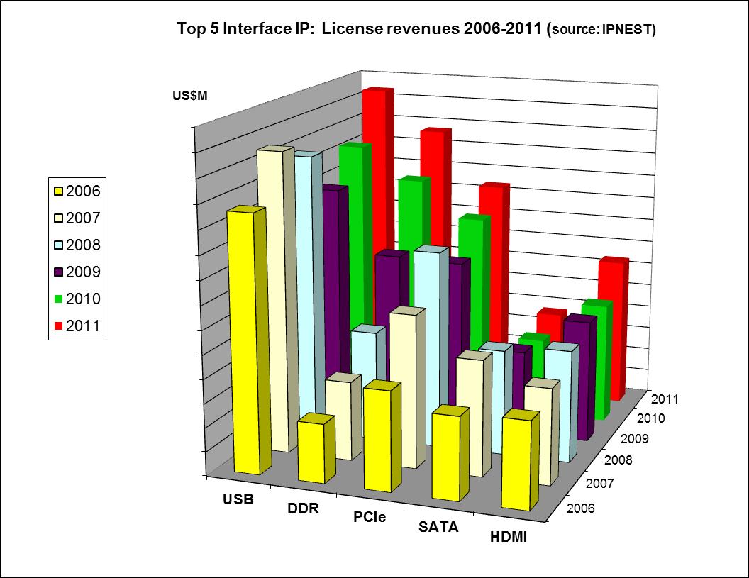
What type of information could be found in the survey, and in the latest version, the 4[SUP]th[/SUP], issued these days? In fact, IPNEST is not only providing the market share information, protocol by protocol and year by year for 2006 to 2011 (when relevant), but do a real research work, in order to answer many other questions, which are the questions you try to answer when you are Marketing Manager for an IP vendor (I was in charge of this job for IP vendors), or when you are in charge of the Business development for an ASIC (Design Service or Foundry) company (that I did for TI and Atmel a while ago), or when you need to take the make-or-buy decision when managing a project for an IDM or fabless chip maker – and if the decision is finally to buy, who should I buy and at what price? The type of answers IPNEST customers find in the “Interface IP Survey” are:
- 2012-2016 Forecast, by protocol, for USB, PCIe, SATA, HDMI, DDRn, MIPI, Ethernet, DisplayPort, based on a bottom-up approach, by design start by application
- License price by type for the Controller (Host or Device, dual Mode)
- License price by technology node for the PHY
- License price evolution: technology node shift for the PHY, Controller pricing by protocol generation
- By protocol, competitive analysis of the various IP vendors: when you buy an expensive and complex IP, the price is important, but other issues count as well, like
- Will the IP vendor stay in the market, keep developing the new protocol generations?
- Is the PHY IP vendor linked to one ASIC technology provider only or does he support various foundries?
- Is one IP vendor “ultra-dominant” in this segment, so the success chance is weak, if I plan to enter this protocol market?
These are precise questions that you need to answer before developing an IP, or buying it to integrate it in your latest IC, in both cases you’re most important challenge, whether you are IP vendor or chip maker. But the survey also address questions, for which a binary answer does not necessarily exist, but which gives you the guidance’s you need to select a protocol, and keep sure your roadmap will align with the market trends, and your customer needs. For example, if you develop for the storage market, you will not ignore SSD technology. But, when deciding to support SSD, will you interface it with SATA, SATA Express, NVM Express or homemade Nand Flash controller? Or, if you develop a portable electronic device for Consumer electronic market, should you jump start integrating MIPI technology now? For many of these questions, we propose answers, based on a 30 years industry experience, acquired in the field… That’s why also we have built for each survey a 5 years forecast, based on a bottom-up approach, that we propose with a good level of confidence to our customers, even if we know that any economic recession could heavily modify it.
You probably better know why IPNEST is the leader on the IP dedicated surveys, enjoying this long customer list:
For those who want to know more, you can read the height pages Introduction, extracted from the 4[SUP]th[/SUP] version of the “Interface IP Survey”, issue in August 2012, and proposed to Semiwiki readers very soon here.
Eric Esteve from IPNEST –
Table of Content for “Interface IP Survey 2006-2011 – Forecast 2012-2016” available here