Recently, Forte Design Systems announced the release of a new core engine to their popular high-level synthesis tool offering. It is a large undertaking, so I asked John Sanguinetti, Forte’s CTO, to answer some questions about that development effort.
Q. How long has it been since the last major upgrade of the Cynthesizer engine (when was C4 released)? Why are you doing this now?
A: This is the first major architectural change to the Cynthesizer core since our initial release in 2001. Of course we’ve been updating and improving the core along the way but it is the first time we’ve changed the architecture. We’ve known for a few years that our current platform would only take us so far and that we would need an upgrade. We started on that process a little over 2 years ago and over the last 18 months it has been one of the top priorities.
Q. What are the major changes in the engine? How will users benefit?
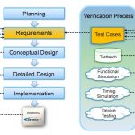
A: The biggest change is that we’ve combined the scheduling and allocation phases. High-level synthesis research for some time now has focused on combining scheduling and allocation. While our previous core organization worked pretty well in general, there were a number of optimizations that we identified that we really couldn’t do with our previous organization. With C5, we can now implement these new optimizations.
More importantly, it provides users with a more predictable platform. The tool can now quickly and thoroughly evaluate changes to the schedule, push them all the way through allocation (where parts are assigned and shared), and get a much more detailed view of the resulting RTL circuit.
We’ve also been able to deliver our first user-controlled power features on the new platform. Cynthesizer has had passive low power features for some time that included low power coding styles, known-good architectures for low power, and choice of half- and quarter-speed memories, for example. Cynthesizer 5 adds the ability to trade-off either area or performance for lower power. New features include integrated HLS-optimized clock gating, FSM (finite state machine) optimization to minimize datapath logic switching, and memory access optimizations. Using Cynthesizer’s exploration capabilities, it will be easy to get multiple QoR data points quickly.
We’ve also developed a new SystemC IDE and analysis environment. The goal with this product is to allow new users to more easily move to SystemC-based design. At the same time we wanted to make it easier for Cynthesizer experts to quickly analyze designs to get to their desired results more quickly. It’s a careful balancing act but we are confident that it is going to be a significant new feature.
Q. How much effort was involved in development? Quality assurance?
A: It was a big effort taking the better part of 2 years with most of our staff. As you know, we’ve been delivering production-level high-level synthesis for more than 10 years and in that time we’ve built up an extensive regression suite. Our regression suite is made up of nearly 10,000 designs that range from small unit test cases to customer-deployed designs with millions of gates. This has proven to be a big advantage for us throughout the development of Cynthesizer 5 because we were able to quickly see the trends in terms of area, performance, and power.
Q. What was the greatest engineering challenge in making C5?
A: Whenever you deliver new technologies into an existing customer base the first challenge is to make sure that your existing customers see the new benefits without giving up anything on their existing designs. This is actually harder than it sounds. One of the toughest challenges is that Cynthesizer 4.3 can achieve really good results already. Getting the quality of results (QoR) to be better in every case was a tall order, but we have very nearly achieved that. The end result is that existing customers should have a great experience with Cynthesizer 5 with no disruption in their flow and both new and existing customers will find some really exiting new features that further differentiate Cynthesizer.
Q. Were any customers involved in C5? If so how many and how (and who if you can tell us)?
A: We always work closely with customers on any new developments. We had partners in the US, Japan, and Korea looking at Cynthesizer 5 very early on as well as Cynthesizer Low Power.
Q. What effort should current users expect in transitioning to C5?
A: We don’t expect any significant effort for existing users. We’ve included compatibility modes to make sure that the transition is easy with existing designs.
Q. What are the next major improvements to the engine? Will those be a focus of C6 or will you be able to add those features into C5?
A: We’ve designed this platform to be able to carry the product line for a long time. We expect to be spending a lot of time continuing to raise the abstraction-level of the input, adding new low-power optimizations, and expanding our IP effort.
Q: What will Forte be showing at DAC in Austin?
A: Cynthesizer 5 will be the main focus but we will also have a number detailed technical sessions. One of customers, Adapt-IP, will be showing a USB 3.0 design completely designed with Cynthesizer running on a live board. We’ll also have a joint session with Ansys Apache on low power and a detailed technical tutorial on Cynthesizer. You can find more on our website at www.ForteDS.com/dac2013.
lang: en_US