llmda newsletter ad (2)

Towards the 0 DPM Test Goal

Towards the 0 DPM Test Goal
by Paul McLellan on 07-10-2013 at 10:43 am

At Semicon yesterday I attended Mentor’s presentation on improving test standards. Joe Sawicki was meant to present but he was unable to get a flight due to the ongoing disruption at SFO after last weekend’s crash. I just flew in myself and it is odd to see the carcase of that 777 just beside the runway we landed on.

The big challenges facing manufacturing test at present are:

  • achieving adequate test quality
  • minimizing test cost
  • dealing with increased design size and resultant test complexity
  • methodology and tools for testing 3D stacked die
  • ramping production and yield quickly


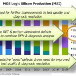
Over the last few process generations, changes in the manufacturing technology have had knock-on effects on test. First back at 180nm with damascene copper interconnect there was an increase in resistive “open” defect requiring improved test quality. Then at 45nm and below the aggressive RET decoration created pattern dependent defects requiring DFM and diagnosis to be more tightly combined. And now with FinFETs, we require further improvements in test quality and diagnosis.

Some safety critical applications such as automotive are starting to have 0 DPM (defects per million) as a quality requirement. This is obviously not appropriate for all designs: tripling the test cost for chips for cell-phones for example is the wrong trade-off. But another area requiring high test yield is for die going into any sort of 3D stack. A bad die getting through doesn’t just waste that die (and it was bad anyway), it wastes several good die and an expensive package.


The new processes, FinFET and FD-SOI are still too new to really understand how defects will behave in new cells. But people are anticipating increased in-cell defectivity since there is a dramatic reduction in the minimum feature size for FinFETs compared to planar devices.

In the past, most test coverage has been based on stuck-at fault models. This assumes that a test is good if it detects whether the output of a cell that is stuck at 0 or stuck at 1 causes the test to fail. Everyone knows that this is not really a realistic model of all ways that chips actually fail but it has been surprisingly robust and it is easy to measure.


But with more complex processes (and RET and more complex failure modes) this is not enough. The first thing to do is to look inside the cells and use cell-aware ATPG to look for undetected faults based on the actual cell layout and transistor netlist structure. One particular problem with FinFETs is strength related defects. Since transistors are a fixed size and multiple fins are used for higher drive, there is the risk that not all the transistors fail and so the drive will not be adequate but the circuit will still be functionally correct.

AMD did some work with Mentor on improving quality using cell-aware ATPG. Compared to just using the regular stuck-at model, they improved test quality at wafer sort by an incredible 885 DPM. This is a huge number. It was high enough to hugely reduce the need for system level functional test.

The next issue is to be able to drill down into systematic failures, where many more chips than expected fail on the same vector. The fix, for example, may be to redo the DFM decoration to improve yield, but that requires the capability to look for pattern-related failures and to isolate the problem not just to a net but to the correct segment of the net.


So in the new era there will be changes in test methodology:

  • need better detection of FinFET defect mechanisms (within the cells)
  • need further improvements in diagnosis resolution and root-cause determination

Obviously with its strong position in test, Mentor plans to deliver the required capabilities in the future.

LATE NEWS:
at 1pm today at Sematech Mentor’s TestKompress with cell-aware ATPG was awarded the Best of West award. The award recognizes important product and technology developments in the microelectronics supply chain. The Best of West finalists were selected based on their financial impact on the industry, engineering or scientific achievement, and/or societal impact.


Apple iOS7 Will Drive The Next Semiconductor Cycle

Apple iOS7 Will Drive The Next Semiconductor Cycle
by Ed McKernan on 07-08-2013 at 12:00 am

We have entered the Summer lull, the quiet period before what is likely to be Apple’s largest volume launch of smartphones ever. While the launches are coming in like clockwork, it is the magnitude of the ramp that is likely to surprise many and it will be due not just to the features of iOS7, but also to the adoption of a well-worn Microsoft strategy. Continue reading “Apple iOS7 Will Drive The Next Semiconductor Cycle”


Intel Versus the Fabless Semiconductor Ecosystem!

Intel Versus the Fabless Semiconductor Ecosystem!
by Daniel Nenni on 07-07-2013 at 7:30 pm

In case you missed it, there is an interesting conversation on my blog, The Future of Mobile Devices and the Semiconductor Landscape!, between Ashraf Eassa and myself. Ashraf and I also converse privately, he’s a very respectful and intelligent young man. For the last year Ashraf has been writing financial articles for Seeking Alpha which has earned him the reputation of an “Internationally Recognized Intel Fan”.

Ashraf did a nice Intel vs TSMC process comparison in the comment section, clearly he put a lot of time into it and for that I’m grateful. It also gives a telling look into how financial analysts think. Ashraf is a recent college graduate, if you are looking for an entry level analyst make him an offer, absolutely. Unfortunately, Ashraf, along with many other analysts, do not GET the fabless semiconductor ecosystem:

How will the fabless players compete at 20nm if they will not get the performance/power improvements to roughly match Intel’s 22nm FinFET process until 2015 when, presumably, Intel will be shipping its 2nd gen FinFET? Perhaps I’m missing something…

Let’s start at the beginning, the fundamental reason the fabless semiconductor ecosystem exists today is because traditional semiconductor companies did not do their job. They did not have vision, they did not innovate, and most importantly they did not efficiently manage their manufacturing capabilities. The first fabless companies leveraged excess semiconductor manufacturing capacity out of Japan innovating their way into new markets. Chip and Technologies was one of the first and they schooled Intel on how to build PC chipsets. Intel deployed the “if you can’t beat them buy them” strategy and the rest is history. Another early fabless innovator is Xilinx.

It is a familiar Silicon Valley story, Xilinx co-founder Ross Freeman wanted to create a blank semiconductor device that could be quickly programmed based on an application’s requirements. Even back then semiconductors cost millions of dollars to design and manufacture so this was not only a cost savings, FPGAs also dramatically reduced time to market for electronic products. Of course Ross’s employer Zilog did not share this vision and Xilinx was created in 1984. The founder of Zilog was an ex Intel employee who spun out to compete with his employer so he had vision. Unfortunately he had microprocessor blinders on and could not see the big picture. Sound familiar (Intel)?

Fast forward to today, the mobile market owns the semiconductor industry with SoCs driving process technology. The traditional semiconductor companies that once opened up their manufacturing services to the fabless companies are now fab-lite or totally fabless. Intel is also now renting out manufacturing capacity and looks to compete with the top fabless companies for mobile sockets with its Atom processor and superior manufacturing technology. Looks good on PowerPoint, as Ashraf has power pointed out, but the history of the semiconductor industry does not agree.


The mobile SoC market is fast moving and Intel is not. Qualcom and Apple alone ship more SoCs than Intel ships processors and at a much lower cost/margin. Qualcomm and Apple both license the ARM architecture and custom tailor their processors to the mobile products they control. Samsung is also licensing the ARM architecture for their line of SoCs. It’s not just a power/performance/price play, it also allows a much higher level of device integration. I don’t EVER see Intel becoming an IP company and licensing the Atom architecture.

The definition of SoC is System on Chip which means all of the semiconductor devices inside your phone will be on one chip at the lowest possible cost/margins. This will require mobile vision, flexibility, and a fast moving product plan. Does that really sound like Intel to you?

lang: en_US


4th Fundamental Circuit Element – Can it be a boon to Semiconductor Industry?

4th Fundamental Circuit Element – Can it be a boon to Semiconductor Industry?
by Pawan Fangaria on 07-07-2013 at 1:11 pm

It was a nice break after my vacation, indulging into some of the pure science stuff, when an old colleague of mine, Dr. Gaurav Gandhi, founder of mLabs in Delhi came across introducing me to his new research and possible developments in this field. Gaurav was actually in my product validation team while I was at Cadence, very passionate about getting deep into technology and doing things in newer ways.

I was delighted to know details about Memristor, about which I didn’t have full knowledge.

Gaurav and Varun Aggarwal have published a paper “Bipolar Electrical Switching in Metal-Metal Contacts” at Cornell University Library. One can also access it from their website here. Memristor was first discovered by Prof. Leon O. Chua (University of California, Berkeley) in 1971 as a non-linear passive two-terminal electrical component linking electric charge and magnetic flux. Later in 2008, Stan Williams, et al. from HP Labs discovered memristor which exhibits electrically controllable state-dependent resistance. HP Labs actually developed memristor using thin titanium dioxide film between two electrodes. More historical references can be found in Gaurav’s paper, but let’s see what his paper tells us and then ponder over a very near term opportunities and developments in this direction.

Gaurav actually discovered memristive properties in cat’s whisker (one of the first wireless radio detector) as well and identified the state variable governing the resistance state of the device which can be programmed to switch between multiple stable resistance states. He also emphasized on memristive properties being available in larger class of devices called coherers (including cat’s whisker), hence introducing canonical implementation of a memristor.

[Cat’s whisker setup]

In his experimentation, cat’s whisker setup was achieved through Galena crystal in contact with Phosphorous bronze wire, currents of varying amplitudes were passed through and voltages across the setup were recorded. He developed a programmable system in which input current waveform of desired amplitude and time period could be digitally generated and output voltage waveform recorded.

Results of two representative input waveforms – i) Rising triangular bursts of currents and ii) Fixed triangular waveforms in both positive and negative directions, show that the devices exhibit three distinct behaviours: i) cohering action, ii) multi-state memristive behaviour and iii) bi-stable resistive RAM (Random Access Memory) behaviour. Other than this setup, this phenomenon was observed in wide class of crystals like Carborundum, Iron Pyrite and metals including Iron filling, Aluminium, Ni etc. A coherer is comprised of imperfect metal-metal contact.

[Current and voltage Vs time and device behaviour as state-dependent resistance]

It can be clearly inferred that at a current higher than a threshold, average resistance of the device falls. Once the device takes this new state, it maintains its non-linear DC resistance even on excitation by a current value of less than that threshold, that’s an indication of cohering action.

It’s also evident that the maximum current during a time interval acts as a state variable, dictating the resistance in that time interval. As the device experiences higher peak currents, it sets itself to lower non-linear DC resistance values. This shows multi-state behaviour of the device.

[Alternate current and voltage Vs time and bi-stable memristive behaviour of device]

When activated by a bipolar current input, the device sets itself in one state in the positive cycle and in a different state in the negative cycle, thus oscillating between these two stable states, forming the famous eight-shaped pinched hysteresis loop in its V-I characteristic. That’s the bi-stable resistive RAM behaviour.

Opportunities To Semiconductor Industry – It’s clear that a piece of wire can be configured as a memory component which can be ultra optimized in terms of PPA (Power, Performance and Area), the most sought after criteria in semiconductor industry today. It can work great as storage devices. Considering its multi-state property, I can foresee that there could be more applications. Also, once commercially proven, I believe its manufacturing could be simpler and cost effective, if a ubiquitous and suitable material with these properties could be utilized.

As stated above, HP Labs had experimented with memristors. They, in collaborations with Hynix, are said to have plans to manufacture ReRAM (Resistive Random Access Memory) commercially which can replace Flash memory used in smart phones, tablets and MP3 players. Possibly, HP can unveil its baby by the end of 2014.

I am looking forward to more such applications of this simple but far reaching device. Comments and suggestions are welcome!!


Should an IP vendor become a PHY IP Dealer?

Should an IP vendor become a PHY IP Dealer?
by Eric Esteve on 07-07-2013 at 3:20 am

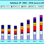
This is not a theoretical question. Imagine that you are developing and selling digital IP, like Interface Controller, PCI Express or USB 2.0 or 3.0, or MIPI Camera Serial Interface (CSI) or Display Serial Interface (DSI). If you look at companies like Synopsys, they have built their success on the “Integrated Interface IP” concept. In other words, they sell both the Controller and the PHY IP to support a specific protocol (USB, PCIe, MIPI etc…). You may think that you could much better developed your business by mimic competition, and be able to sell both the Controller and the PHY IP. The first problem you are facing is finding right resources: if you can easily increase your digital development design team, it’s much more difficult to find, then attract and hire experienced Analog designers (I mean those able to design a 6 GHz PLL or a 10 Gbps SerDes). Thus, it looks easier and faster to simply resale PHY IP developed by another party…and gets a higher share of this fast growing market, Interface IP:

After some research, you have exercised your network, and find, for example an IDM ready to run a partnership with you: he brings the Silicon validated PHY IP, you bring your support team and sale network and market these IP. No doubt that you will find such an IDM, as some of them have to increase their revenue to compensate some sale weaknesses. Let’s try to draw the complete marketing figure, and see the pros, and also the drawbacks linked with such a case.

The first positive point, I should say very positive, is the fact that this very complex IP (say a 5 Gbps SerDes for example) has been not only Silicon proven, but also Production and system proven. This is a very strong sale argument, and you will certainly use it. Nevertheless, don’t forget that this argument will stay valid only in the same technology case: same technology node, same foundry. As soon as you would need to port the IP, either in another technology node from the same Silicon foundry, or to another foundry similar technology node, you will have to modify the design, thus opening the door to any potential mistake… By the way, who in your team will take care of this porting? In fact, you will have to hire a few of these analog designers. From a past experience, being ASIC program manager for a SoC including several complexes analog functions, these functions being responsible for a 18 month additional delay, leading to successive Silicon ending to a “K” version (think A is the first, then B and so on), my personal advice is to hire the best you can find!

Another drawback comes to my mind: if you resale these IP from this IDM, there is a pretty high probability that other IP vendors will deal these same IP, coming from the same source. Then, you face another issue, which is the lack of differentiation. You become the Nth IP vendor selling the exactly same product. Some old marketing training reminds me that, in this case, you will probably have to use price as the unique possible differentiator. Price differentiation is the worst situation when selling a complex function! Such a differentiator works well when selling commodities like TTL or DRAM. The only way to escape this situation is to rely on an efficient and talented analog design team, so you can redesign the function for lower power, smaller area or better performance. But, in this case, why not design your own complex IP, so you have the complete knowledge of the function, being in the position to give the best possible technical support, or modify the IP upon customer request (and finally creating much more value) ? And last but not least business related argument, your sales team will market a “clean” IP, from a legal standpoint, as you completely own the IP rights… Just make your decision and choose to be a PHY IP dealer, or if it’s better to develop and license your own IP.

By Eric Esteve from IPnest

lang: en_US


Calypto 2013 Report

Calypto 2013 Report
by Paul McLellan on 07-05-2013 at 5:48 am

Each year Calypto runs a survey of end-users. This year’s survey and report has two parts, power reduction and high level synthesis (HLS).

The topics covered are:

  • survey methodology and demographics
  • top methods used to reduce power
  • engineering time spent on specfiic RTL tasks to reduce power
  • plans to deploy RTL power reduction tools in 2013
  • methods to verify HLS output RTL
  • important technologies to implement with HLS
  • summary


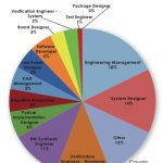
The above pie-chart shows the detailed breakdown. The primary job functions specified were engineering and CAD management (23%), system designer (14%), verification engineer – hardware (12%), and hardware synthesis engineers (11%).

I’m not going to go into the whole report here, you can download it and read the whole thing. But I’ll pick out a couple of interesting charts.


The first one shows the popularity of the main means of power reduction. This is at the RTL level so some techniques for power reduction are applicable only at other stages in the design process.

  • Top is sequential power gating (such as is done by PowerPro and its competitors).
  • Power gating, which is powering down blocks that are completely unused, such as the transmit/receive logic in a cellphone when there is no call taking place
  • Third is combinational clock gating. I think this is so universal that people don’t always realize they are using it since synthesis does it semi-automatically, so I’m surprised it isn’t #1. It usually is in this sort of survey.
  • Next is dynamic voltage and frequency scaling (DVFS) which is surprisingly high to me. It is a difficult technique to use requiring careful tuning of how fast and in what order the frequencies and voltages are changed. It is used in high end microprocessors but I’ve not really heard of it in other parts of big SoCs
  • Next is multi V[SUB]th[/SUB], again a relatively low score if it covers using multi V[SUB]th[/SUB] libraries. RTL synthesis does this automatically so many people may be unaware they are doing this even when they are.
  • Resource sharing, memory gating and data gating bring up the rear.


Interestingly, the chart above shows which techniques are used to verifying high level synthesis RTL against its original input doesn’t have a lot of people using sequential formal verification, which I find a bit surprising. FPGA prototyping seems a poor substitute for formal techniques. After all, for RTL synthesis we pretty much use formal techniques rather than simulation these days. Anyway, since Calypto has the only sequential formal verification tool on the market today, that is a potentially high growth opportunity.

So in summary, SoC, IC, and FPGA design professionals completed a blind, anonymous survey online.

  • The average time spent on various RTL power tasks was: 20 percent on automated optimization, 20 percent on guided/manual power reduction, and 17 percent RTL power analysis.
  • The combined total organizational involvement with using, implementing, or evaluating RTL power reduction technology is close to two-thirds. Almost a quarter of respondents said their organization had already implemented RTL power reduction tools.
  • More than three-quarters of respondents used HLS. The top method for verifying the RTL output was FPGA prototyping. There was a range of usage among directed tests, assertion-based, constrained random, hardware emulation, and C-to-RTL formal.


GSA Awards Deadline Looming + GSA Entrepreneurship Conference

GSA Awards Deadline Looming + GSA Entrepreneurship Conference
by Paul McLellan on 07-05-2013 at 5:09 am

GSA has award for various categories that are presented at their annual awards dinner. This year’s dinner will be on Thursday December 12th at the Santa Clara Convention Center.

Some of the awards have now passed their cutoff date. But a few remain open until July 12th (hurry, just one more week):

  • Startup to Watch Award
  • Most Respected Private Semiconductor Company Awards
  • Outstanding Asia-Pacific (APAC) Semiconductor Company Award
  • Outstanding Europe, Middle-East, Africa (EMEA) Semiconductor Company Award

There are also several awards for public companies:

  • Best Financially Managed Semiconductor Company
  • Most Respected Public Semiconductor Award (>$1B sales)
  • Most Respected Public Semiconductor Award ($251M to $1B sales)
  • Most Respected Public Semiconductor Award ($100M to $250M sales)
  • Analyst Favorite Semiconductor Company Award

Public companies do not need to be nominated since they are assessed based on public financial data. But private companies and individuals do need to be nominated on one of these forms.

If you want to attend the dinner (either as an individual or as a company purchasing a whole table) then the details are here. The dinner is made possible by sponsor TSMC as well as some other general sponsors. December 12th at 7pm, Santa Clara Convention Center.

The keynote speaker at the dinner is Cory Booker, the mayor of Newark NJ.The Honorable Cory A. Booker is the Mayor of Newark, New Jersey. He took the oath of office as Mayor of New Jersey’s largest city in July 2006 following a sweeping electoral victory, and was re-elected for a second term in another overwhelming majority in 2010. Mayor Booker brings his passion for social change to the podium. Sharing stories informed by real life, Mayor Booker demonstrates the need for everyone to take responsibility to help this nation live up to its promise. Mayor Booker also sheds light on the necessary reform government needs to undergo to become equipped to deal with the challenges of modern times. Drawing from a deep belief in service and social justice, Mayor Booker inspires audiences to greater civic responsibility and issues a call to action for America.

Full details of all the awards, including the small print (“must be a semiconductor company” etc) are on the GSA website here. This is also where you can find links to the nomination forms.

Also, don’t forget the annual GSA Entrepreneurship Conference is at the Computer History Museum on July 18th. It is from 3.30pm to 8.30pm (note the slightly unusual time). Details are here. There is no charge but you must register. The full program, including details of the panels and the speakers is here.


Should the Design Automation Conference Colocate with SEMICON West?

Should the Design Automation Conference Colocate with SEMICON West?
by Daniel Nenni on 07-03-2013 at 8:10 pm

My friend and fellow blogger Kurt Shuler wrote recently, “DAC Is Dead? Long Live DAC!”, which is worth a click over. In addition to providing a nice attendance graph and the top three reasons why it is NOT all rosy, Kurt suggests colocating DAC with other conferences (DESIGN West) but fails to mention SEMICON West.

SEMICON West is the flagship annual event for the global microelectronics industry. It is the premier event for the display of new products and technologies for microelectronics design and manufacturing, featuring technologies from across the microelectronics supply chain, from electronic design automation, to device fabrication (wafer processing), to final manufacturing (assembly, packaging, and test). More than semiconductors, SEMICON West is also showcase for emerging markets and technologies born from the microelectronics industry, including micro-electromechanical systems (MEMS), photovoltaics (PV), flexible electronics and displays, nano-electronics, solid state lighting (LEDs), and related technologies.

More than 30,000 people routinely attend SEMICON West compared to DAC’s 7,000 or so. Take a look at SEMICON’s event calendar and see the synergy for yourself. Here are some of the EDA specific talks:

Even more interesting, GLOBALFOUNDRIES CEO lands the opening keynote with Foundry-driven Innovation in the Mobility Era:

The Mobile Era is clearly upon us. Mobile devices are outselling PCs. More people access the internet through their phone or tablet than their desktop. Semiconductor consumption by mobile applications surpassed that of PCs last year for the first time. What does this all mean to the electronics industry, and the semiconductor infrastructure that supports it?

The Mobile Era introduces new challenges and new types of players. A much more complex and interconnected ecosystem defines this new reality, and companies are jockeying for position to align with the right partners and technologies.

At the semiconductor level is it clear that the old manufacturing model won’t support the needs of this dynamic new landscape. The foundry-based model, which has spurned so many fabless success stories over the past two decades, will continues to be a key driver behind this mobile revolution, and in fact will assert more influence and innovation than ever before. As successful as this approach has been, like all living organisms, especially those in electronics, we have to continue to evolve. Clearly, we must change – Call it Foundry 2.0………

Which is followed by several more GF presentations:

Looking good SEMICON West, I would colocate with you anytime! I hope to see you all there!

lang: en_US


Easy SystemC Debugging

Easy SystemC Debugging
by Randy Smith on 07-03-2013 at 7:00 pm

Electronic system design has been slowly migrating to higher level languages such as SystemC for more than a decade now. SystemC is an open source C++ library that has emerged as a standard for high-level design and system modeling. Writing code in SystemC has several advantages which I won’t elaborate on in this article, though if you want more information note that searching for “SystemC Tutorial” (in double-quotes to get that exact phrase) you get more than 3,000 hits on Google. Forte also offers a free SystemC training course. As a former programmer myself, I am interested in the tools and environment the programmers have to use in working in a particular language. While Forte is best known for its high-level synthesis capabilities, I was pleasantly surprised at the environment Forte has delivered for SystemC debugging.

Forte recently announced their YouTube channel where anyone can simply go and watch video created by them. Interestingly, the professional looking videos I have viewed there seem to be moderated by Forte’s CEO Sean Dart. His light Aussie accent should be easy enough for all English-speakers to understand and the clearly Camtasia-developed videos are very nicely edited.


Forte’s Cynthesizer Workbench works with multiple panes which easily allow you to see the source code, call stack, variable values, and list of breakpoints, all at the same time. From this environment you can see the variable values in the context of each procedure (function) on the stack. This is nicely displayed for more complex variables as well, such as showing the fields in a record pointed to from a local variable. In the source code pane you can easily set breakpoints as well as control execution using tool icons to step into or out of loops. Another useful feature is the ability to skip over specific lines of code.

The simulator is invoked directly from within the design/debug environment and you can optionally select the simulation configuration to use for your session. There is a compilation step which is automatically invoked prior to simulation if the code has changed. The loop of setting breakpoints, simulating, analyzing, editing, and re-simulating is all contained within the environment. Also, Forte supports many third-party tools within its flow (a list is available here). This environment is indeed complete for all of the basic debugging needs.

If you are making the move to a higher-level language or if you like to see a clean, useful debugging environment for SystemC development, I suggest you take a look at Forte’s video page for more information. There you will find videos on high-level synthesis, Cynthesizer Workbench, SystemC tutorials, and demo examples. For fun you can even check out the video of the DAC closing bagpipes performance which Forte has sponsored for several years now.

lang: en_US


Free Pass to SEMICON West!

Free Pass to SEMICON West!
by Beth Martin on 07-03-2013 at 1:00 pm

SEMICON West is next week, July 9-11 in San Francisco. If you haven’t signed up, and want to attend for free instead of $100,

1) Send an email to silicon_test@mentor.com with subject line “Semicon pass.”
2) Register for SEMICON West
3) After registering, download the SEMICON West mobile app and start building your schedule. Here are some suggestions:
.

  • Interested in transistor architectures below 20nm? Attend this session in the South Hall TechXPOT on Tuesday from 10:30-12:30: “Leveraging Nonplanar Transistor Architectures and New Materials to Power Mobility Apps Beyond 20nm.”The line-up of speakers in this one is stellar. Joe Sawicki, VP and GM of the Design-to Silicon Division at Mentor Graphics will talk about cell-aware test, which will be vital to FinFET yield ramp.
    .

  • After that, headover to the North Hall TechXPOT for “Semiconductor Test: Smarter, Faster, More Productive” from 1:30-4:00pm. Each of the six speakers in this moderated session will explore the latest trends and developments to improve yield, advances in probe card technology, adaptive test integration, and 3DIC test.
    .

  • For an in-depth discussion of cell-aware test for FinFET, visit the North Hall TechHUB on Tuesday at 2-3pm. Steve Pateras of Mentor Graphics can tell you everything you want to know. The TechHUBs are new this year, and are designed for interaction between the presenter and audience, so don’t be shy with your questions.
    .

  • Wednesday 2pm-3pm, in the Executive Panel “A Promising but Challenging Future,” Mentor Graphics CEO Wally Rhines and four other industry executives discuss the outlook for semiconductor manufacturing.

.

And while you’re there, stop by the Mentor Graphics booth 6245 and sign up to win a JAMBOX Bluetooth Speaker. See all Mentor activities at SEMICON West.