Last year at DAC I visited this little-known physical IP company called DXCorr, so I decided to visit them again this year and get an update.
Physical IP Update at DAC


Last year at DAC I visited this little-known physical IP company called DXCorr, so I decided to visit them again this year and get an update.

At DAC in Austin a design company, foundry and EDA vendor teamed up to present their experiences with 14nm FinFETs during a breakfast on Tuesday.
Panelists included:
Continue reading “Deploying 14nm FinFETs in your Next Mobile SoC”
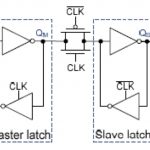
Recently, I discussed the increasing risk of metastability hazards at nanoscale geometries. These risks are significantly aggravated at low supply voltages and low temperatures and must be addressed during the design cycle of any mission critical application. This time I discuss what it takes to estimate a synchronizer’s mean-time between failures (MTBF).
Some flip-flops do a better job as a synchronizer than others. Sometimes you need to cascade flip-flops to get the MTBF your customer’s product needs. As the project manager, how are you going to decide about these issues when the engineer that designed the synchronizer flip-flop is not the engineer that integrates it into your final product?
The engineer that designed your standard-cell synchronizer, call him Sam, should know about his circuit’s settling time constant and its metastability window. In fact, if the synchronizer is a master-slave (often the case), you need to know the settling time constant for the master and the slave, for a total of three parameters:
The engineer that integrates the synchronizer into a product, Ian, knows about the intended clock frequency, the average rate of input data transitions and the clock’s duty cycle.
To accurately estimate the synchronizer’s MTBF, all six of these parameters need to be known to you. Assuming you have them all, for an allowed settling time t, the formula is:
Clearly, the bigger (longer) the allowed selling time t, the better (longer) the MTBF. It’s also clear that t must be less than the clock period by, at least, the setup time of the next stage plus the delay of any logic between the synchronizer output and the next stage input.
The above formula for estimating MTBF is a familiar one except for the factor in the denominator of the exponent that represents the effective value of the settling time constant.
When the master and slave settling time constants are equal, then they both equal the effective settling time. This is true no matter the duty cycle. When the two settling time constants are not equal, the duty cycle can make a big difference in the settling time behavior. The duty cycle is usually around 0.5 and cannot vary too much without violating the clock minimum pulse-width constraint. However, for large differences in settling time constants, the duty cycle must be considered since it affects the exponent in the MTBF formula.
So both Sam and Ian each know three of the parameters that go into the MTBF estimate. Sam should specify his parameters at the worst-case corner: Typically SS, low-supply-voltage and low-temperature as specified by Ian for the product’s operational environment. Ian then specifies his parameters and calculates t and MTBF.
There are two novel issues that have appeared in this discussion. First, the effect of clock duty-cycle on MTBF has, until recently, been overlooked, but can be included by having the synchronizer’s standard-cell vendor specify the settling time constants of both the master and slave. Second, when it comes to synchronizers, standard-cell designers (Sam) and integrators (Ian) each have only half the MTBF story. They must work together to produce safe products for mission critical applications. The resulting products are neither over-designed nor unreliable. The Blendics metastability analysis tool, MetaACE, can help synchronizer vendors provide reliable parameter sets to their customers.
Increasingly, at nanoscale geometries, a single-stage synchronizer will not do the job that your customer wants and a multistage synchronizer is required. In Part 2 of this topic I will discuss the issues associated with estimating MTBF for these synchronizers (here is a hint: most published methods are not very good).
lang: en_US
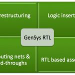
Increasingly, SoC designs consist of assembling blocks of pre-designed IP. One special case is the derivative design where not just the IP blocks get re-used but a lot of the assembly itself. For example, in the design below some blocks are added, some blocks are updated, some hierarchy is changed. But the bulk of the design remains unchanged from the original to the derivative. The trick in doing a derivative design is to disturb the original design as little as possible so that you don’t have to rework anything that you (or your colleagues) did previously in the original design.
Doing a derivative design allows efficient re-use of an existing platform, can be done in a comparatively short time and at a much lower cost. Reusing most of the platform for a number of derivatives makes the return on the original investment much more attractive, as pointed out by Gary Smith. A good example of a derivative design is Apple’s A5 chip for the iPad which was clearly an A4 chip with some incremental changes such as a 4 core rather than a 2 core Imagination GPU.
Obviously for a derivative design like this you want to leverage the original design as much as possible and are not going to start from scratch. You’d like to have a tool that helps you manipulate the design at the block level, adding blocks, restructuring logic and so forth.
Atrenta’s GenSys is just such a tool. It allows for RTL restructuring, logic insertion, rerouting nets and feedthroughs and RTL-based assembly. To learn more, next Thursday, June 27th at 9am, Bernard Murphy the CTO of Atrenta will be presenting a webinar RTL Restructuring for the Rest of Us. The webinar will last 30 minutes.
Dr. Murphy has over 25 years experience in design, sales, marketing and business development. He previously held senior positions with Cadence Design Systems, National Semiconductor and Fairchild. Dr. Murphy received both a Bachelor of Arts and D.Phil. in Physics from Oxford University.
Details, including a link for registration, are here.
The growing amount of electronics within today’s automobiles is driving very high quality and reliability requirements to a widening range of semiconductor devices. At the same time, traditional fault models are becoming less effective at achieving desired silicon quality levels. Improvements in test solutions are needed not only to maintain very high quality levels in more advanced technology nodes, but to also address the increasing reliability requirements defined within the ISO 26262 standard.
A new seminar from Mentor Graphics’ Semiconductor Test Solution group explains the latest approaches in testing automotive semiconductors. It will cover details of the new cell-aware test methodology, whichmodels and targets defects within each cell, addressing the inherent limitations of traditional testing. Call-aware testing has been shown to significantly reduce DPM levels in shipped devices.
The seminar will also cover the cell library characterization flow, which creates new cell-aware fault models and is a key element of this methodology. Pattern and coverage results for several industrial designs will be presented as well as silicon test results gathered from several million parts. Cell-internal diagnosis and physical failure analysis results will also be demonstrated to show how cell-aware tests can help detect the root cause of physical defects.
To further expand your test repertoire, the seminar will also cover the IEEE P1687 (IJTAG) standard and how it can help you test the increasing number of digital and mixed-signal embedded IP blocks. Finally, it will describe new hybrid ATPG compression plus logic BIST technology that provides more efficient defect coverage and the ability to apply tests within the system for long-term reliability.If you care about test costs, outgoing product quality levels, diagnosis of semiconductor failures, or maintenance of cell libraries, this seminar will provide you with valuable new approaches to address your testing challenges. June 25 (NA), 26 (Calcutta), 27 (Berlin). Register here…

One of the most challenging stages in an SoC design is achieving timing closure. Actually design closure is perhaps a better term since everything needs to come together such as clock tree, power nets, power budget and so on. Changes made to the design are known as ECOs (which stands for engineering change orders, a term that comes from the days when circuit boards would have colored wires added to address problems, try that on a 20nm chip). Some ECOs are minor timing changes but some are more significant and require RTL changes. This stage of the design cycle can take weeks, with multiple ECO cycles each of which requires many engineers for a few week.
The challenge with ECOs is two fold. First is to avoid the whack-a-mole problem whereby each change fixes one problem and creates two new ones in areas that were previously clean. This problem means that ECOs have to be handled incrementally and intelligently. The second problem is keeping all the views of the design in synchrony.
Keeping the views in synchrony is more difficult than it seems since the RTL may need to be altered to reflect the change. This is called a functional ECO, perhaps coming about due to a spec change or perhaps due to a late discovered issue in verification. But the entire design cannot be re-synthesized, re-placed and re-routed or the timing will never close. But ensuring that just those nets that need to be reworked are the ones that do get reworked is a challenge. Guaranteeing that this is done correctly requires the changes to be verified formally, but to completely re-verify a large design takes a lot of time and compute power.
Today Synopsys announced Formality Ultra which is aimed at precisely this problem and reduces the time taken to handle functional ECOs by a factor of two. It uses formal techniques to analyze mismatches between the (new) RTL and the (old) netlist of the design and so allows the designer to zoom into which changes are needed to implement the ECO. In addition, a new multi-point verification technology quickly checks multiple changes made to the design and so lets designers verify the correctness of their ECOs in a matter of minutes even on multi-million instance designs.
By working incrementally, the whole process is much faster than doing a full verification of the whole design from scratch. Then, to actually make the changes, Formality Ultra generates scripts for IC Compiler to use the incremental P&R capabilities there.
Synopsys have made two videos on Formality Ultra:
Antun’s Intro to Formality Ultra Video
Formality Ultra (ECO capability) Demo Video

This completely misleading title is from a Seeking Alpha (SA) article, a stock investment version of the National Enquirer. As I mentioned inA Call to ARMs, fame and fortune seeking SA Authors make a penny per click so sensationalism sells. The article is not worth your time so I will save you the click and skip to the misguided conclusion:
TSMC is a great company that is a leader in the foundry space, but they are trying too hard to appease investors/customers with some of these claims regarding FinFETs. On the January call (before Intel took Altera and likely Cisco (CSCO) from TSMC), the claim was “minimal volumes of 16nm in 2015”. Now, TSMC is trying to pull a FinFAST one on investors and customers by claiming that 16nm will be in production during 2014, totally bypassing the yet-to-ramp 20nm node.I’m not buying these claims, and neither should you.
First, you should know that Cisco is an IBM ASIC customer not a TSMC customer. ASIC customers do the front half of the design while letting the ASIC vendor (IBM) complete the chip. TSMC does not do ASICs, to be a TSMC customer Cisco will have to go through a services provider such as Global Unichip or LSI Logic. IBM is getting out of the ASIC business so Cisco switching to Intel is a smart move. Today Intel does not have the ecosystem required to allow fabless semiconductor companies to use their fabs without training wheels so the ASIC model works for Intel. Seeking Alpha is promoting F.U.D. (fear, uncertainty, and doubt) here.
Second, here is a FinFET update: As a SemiWiki reader you should know that I have spent a lot of time on FinFETs since hearing about them at ISSCC in 2011:
“New transistor designs are part of the answer,” said Dr. Jack Sun. “Options include a design called FinFET, which uses multiple gates on each transistor. Researchers have made great progress with FinFET, and TSMC hopes it can be used for the next generation of CMOS — the industry’s standard silicon manufacturing process.”
Immediately following, I asked friends and co-workers why TSMC did not already have FinFETs on the road map. The answer from the top fabless companies was that changing transistor architecture is a huge risk and the reward of FinFETs was not clear to them at that time. This was back before 28nm when the top mobile designers chose 28nm polyscion over HKMG for the same reason, lower risk. Leading edge semiconductor designers are by nature risk adverse.
Let us not forget where FinFETs came from: Dr Chenming Hu, the father of FinFETs, and this year’sKaufman Award winner. Chenming’s ground breaking work on FinFETs and the BSIM modeling standard were the highlights of his technical achievements. Chenming is a former TSMC CTO and today is a TSMC Distinguished Professor at UC Berkeley. TSMC knows FinFETs, believe it.
Disclaimer: The following FinFET information comes from sessions and private discussions at the 50[SUP]th[/SUP] Design Automation Conference this month, not from Googling around and making foolish assumptions to support my stock positions.
Today the top fabless semiconductor companies have taped-out 20nm designs which will go into production in 2014. 20nm is now ramping, silicon IS correlating (working), I see no barriers to full production in 2014. TSMC estimated that 20nm revenue would start in Q2 2014 but my bet is they are being conservative by one quarter to appease Wall Street. Either way your iPhone6 will have TSMC 20nm Silicon next year, believe it.
FinFETs are also ahead of schedule. Remember, the first version of FinFETs will use the 20nm process so delivering them in one year versus the standard two year new process technology launch is not unexpected or unrealistic to the experienced semiconductor professional. Consider 16nm to be a half node in regards to development time and delivery.
Today the 16/14nm version .5 PDKs (process design kits) are in use by the leading fabless semiconductor companies. The 1.0 PDKs will be released in October with tape-outs shortly thereafter. If the PDK change between version .5 and version 1.0 is minimal, tape-outs will happen in Q4 of 2013 with production/revenue STARTING one year later (just in time for the iPhone7). If the 1.0 PDK has significant changes tape-outs may be delayed to Q1 2014. Keep reading SemiWiki and you will be one of the first to know.
The other interesting FinFET news is that the foundries will most likely offer two versions of the 16/14nm process: a low power version and a version with more performance. From what I understand the transistor thresholds and pitches will be adjusted for performance. Not a big change but hopefully it will get an extra 10% or more speed-up for those who need it.
So again Seeking Alpha is publishing FinFALSE information to satisfy personal agendas of the Authors. Just my opinion of course.
lang: en_US

Interface IP typically consists of multiple layers, most importantly a PHY (level 1) analog (or mixed signal) block that handles the interface to the outside world and a number of levels of digital controllers. The interfaces between all these levels, especially between the PHY and the controller, is often defined by the interface standard. So, in principle, any PHY should work with any controller. Verification IP should work with any block. And so on.
For example in the M-PHY/UniPro stack, the M-PHY occupies L1 but also lives in the entire UniPro stack. The Host Controller Interface for UFS communicates with transport layer at L4.
However the best way to avoid errors is to use the highly structured verification plans, tools and frameworks that have been developed together for digital SoCs and integration-ready IP with all necessary models and views. Companies like Arasan specialize in providing not just the IP blocks themselves but also the entire verification ecosystem.
To make things worse, the standards are constantly evolving. So it is not just necessary to implement the changes and ensure that the firmware, the digital logic and the analog blocks are all compatible with the new revision (and usually upward compatible with older revisions too). It is also important to provide tools for users to validate their semiconductor design.
For example, the next generation of high-performance mobile storage will use JEDEC’s UFS standard. This provides a host controller interface and leverages SCSI protocols and the MIPI standards UniPro and M-PHY. The current versions are UniPro 1.4, M-PHY 2.0 and UFS 1.1 but they are set to revise this summer to UniPro 1.5, M-PHY 3.0 and UFS 2.0. SoC designers simply don’t have the bandwidth to undertake verification of this sort of complexity themselves. They don’t even have the bandwidth to check that components from different suppliers work together cleanly. So the best solution is to acquire a complete product with all the necessary views from a single supplier.
Arasan also develops and markets FPGA based platforms configured for a number of digital and analog IP products. Customers and eco-system partners use these platforms as:
The challenges are especially acute with new standards, or new versions of existing standards, since standard-compliant devices are not immediately available making verification especially tricky. You can’t just go to Amazon and buy a memory card that is compliant to the new standard, only ones that are compliant to the existing mature standards. What is needed is a whole portfolio consisting of the IP blocks, the verification IP, FPGA-based platforms and, perhaps, other specialized tools.
Chip-level validation is hard enough so pre-verified IP subsystems reduce risk and pull in schedules.

Virtual platforms enable software development to take place on a model of an electronic system. What everyone would like is models that are fast and accurate but that is simply not possible. Fast models are fast because they don’t model everything at the signal level. And accurate models get to be accurate by handling a lot of detail that inevitably makes them slow. Carbon’s virtual platform approach gets around this problem using a technology called Swap and Play. This allows the internal state of a fast model to be saved at any breakpoint and an accurate model to then be initialized with that saved state. In effect, the model switches from being fast to being accurate. Not quite as good as being fast and accurate all the time, but the next best thing.
RTL such as Verilog is, by definition, accurate, but it is too slow for software development. Carbon has a second technology in Carbon Model Studio, which takes RTL models and by throwing away a lot of detail speeds them up a lot. But since they started from the canonical RTL of the block they are completely faithful at the external signal level. These are known as “carbonized” models and they are implementation accurate.
In practice these two technologies mean that it is possible to boot an operating system in seconds and then get to the point of interest (perhaps initializing a device driver or handling some subtle power management issue) and then switch to the accurate model. This is still acceptably fast to allow, for example, stepping through the software while inspecting bus transactions or signal waveforms.
But this only works cleanly when fast models are available. These are normally not generated directly from the RTL but rather are usually created by hand. ARM, for example, creates fast models of all their processors and many other blocks, and these are then made available through Carbon’s IPexchange.
With the latest release of Carbon’s SoCDesigner Plus (their virtual platform technology) users can add fabric components and DDRx memory controllers from any vendor (or internal) to a Swap and Play virtual prototype. This makes it possible for many more systems to take advantage of the “boot an operating system in seconds and then switch to accurate debugging”. Previously support of fabric components and memory controllers was more limited, meaning that some systems could not take advantage of Swap and Play and so were too slow for many purposes.
Using design knowledge gained in the compilation process for these fabric components, not only is an implementation-accurate model created as usual but also a high-speed functional model. This model is capable of executing at 100s of MIPS and then being swapped out with the implementation accurate model at any breakpoint to delve deep into the details of the system.
Carbon Performance Analysis Kits (CPAKs) in the IP portal containing fabric components from Arteris and memory controllers from Cadence (Denali) have all been updated with the new Swap and Play technology.

Last Monday at DAC I met with Linda Fosler, Marketing Director at Mentor Graphics to get an update on what’s new with Eldo(Circuit simulator) and Pyxis (custom IC layout and schematic).
Linda Fosler, Mentor Graphics
Continue reading “Eldo and Pyxis from Mentor, DAC Update”