llmda newsletter ad (2)

Test, The Forgotten Step-Child of Semiconductor Design

Test, The Forgotten Step-Child of Semiconductor Design
by Paul McLellan on 08-20-2013 at 7:56 pm

Somehow, when designing a chip it is synthesis and place & route that gets all the attention. But it is no good taping out perfect layout without also having away to test the silicon. Somehow, test just isn’t as glamorous.

On September 10-12th is the International Test Conference which, as usual, is at the Disneyland Hotel in Anaheim. I actually went to the conference once when I worked for Virtutech. One use for virtual platforms is making it easy to configure “hardware” and then test the software without actually having to go and find all the boards and cables that would be required to assemble that configuration together in the real world. One of our first customers, Ericsson, used our software in just this way, and reckoned it would take a week to get all the hardware in one place to configure each base station. And a few Disney princesses brighten up any business breakfast.

But ITC is not primarily about software testing, although that is one aspect since so many systems have a large software load. ITC is the world’s premier conference dedicated to the electronic test of devices, boards and systems, covering the complete cycle from design verification, test, diagnosis, failure analysis and back to process and design improvement.

As usual, Mentor has a big presence at ITC. Firstly, they are in booth 211 where you can find out about:

  • Hybrid TK/LBIST which combines both compression and logic BIST solutions
  • Cell-Aware test for automotive standards such as ISO 26262
  • Unique test solutions for ARM processors and embedded memory IP
  • 3D test for DRAM and logic
  • Hierarchical solutions for large design efficiency and core plug-and-play reuse
  • Automated IJTAG support for plug-and-play infrastructure and pattern generation
  • Layout-aware diagnosis solutions for understanding and identifying yield loss from test data

One of the big changes in test where Mentor seems to be taking the lead is making test aware of layout. In the past, IC test has largely used a stuck-at model which has performed amazingly well considering just what a bad representation it is of what typically goes wrong on an IC. By adding cell-aware and layout-aware diagnosis it is possible to get much better results. And by better, in the test world, that means more parts failing…on the tester as opposed to out in the real world. Mentor presented the technology in some detail at Sematech and I blogged about it here. Indeed, Mentor’s cell-aware ATPG was awarded the Semicon West “Best of the West” award, which is really the best of show award.


As a way to tempt you to take a look at this, I’ll recap that AMD did an experiment where they ran their normal manufacturing test for a part, then they took the chips that passed and ran them through Mentor’s cell-aware test. They got another 885 DPM failing. This is a huge number. If the chip ships 10M units, that is nearly 9000 systems that are not going to fail. Not all would necessarily make it out of the factory as failing systems, but it seems likely that some would. Everyone knows that the cost of a failure in the field is orders or magnitude more than detecting the failure earlier when it just means discarding a bad die.

There are also a number of presentations by Mentor’s customers.

  • Toshiba on hybrid ATPG compression and LBIST together sharing test logic
  • OnSemi on cell-aware test results in automotive
  • LSI on cell-aware test results
  • ASSET InterTech will have a demo and presentation in their booth showcasing interoperable IJTAG L/TAG flows

On Sunday, Mentor is running a tutorial on “Mixed-Signal DFT and BIST: Trends, Principles and Solutions.” Rumor has it that lots of people are signed up, so it is clearly a hot topic and likely to sell out.

ITC itself (and the exhibits) are September 10-12th, but there are tutorials on Sunday, and panels on Monday with a welcome reception in the evening.

Want to know more about Mentor at ITC, it is all here. Want to go to ITC, register here.

iPhone Buyers Are Younger, Richer, And Better Educated Than Samsung Smartphone Buyers!

iPhone Buyers Are Younger, Richer, And Better Educated Than Samsung Smartphone Buyers!
by Daniel Nenni on 08-20-2013 at 5:00 pm

Business Insider does it again, I just love their charts and with this one I agree with the logic 100%. To me this is more about Samsung the company than Samsung products, Samsung really needs to grow up. The negative marketing, the intellectual property thefts, bribery scandals, product dumping, presidential pardons……. Is that what it really takes to be successful in the new world order?


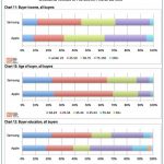
Contrary to Samsung negative marketing, iPhone users are NOT dorks or old people who don’t know any better. The latest data from Consumer Intelligence Research Partners (CIRP) shows it is quite the opposite. According to its survey of smartphone buyers over the last twelve months, iPhone owners in the U.S. are younger, richer, and better educated than the people buying Samsung smartphones. They are much better looking than the average Samsung Galaxy customer too, take me for example!

Seriously, what does it say about a person who does business with a company like Samsung that behaves in such a fashion? Technology over morals? This is a conundrum for me as I shop for my birthday gift, a new 65” plasma TV. Samsung clearly has the best TVs out today in regards to technology and value. Do I take the moral high ground and pay more for an inferior TV? Probably not.

I’m also against mixed smartphone marriages. My entire family has iPhones and iPads and we are living in complete harmony. As I blogged before “Apple v. Samsung: Mixed Phone Marriages End in Divorce?”, I’m just waiting for the studies out of Helsinki that clearly show the majority of divorced families have different brand phones, it’s gonna happen, believe it. And it is not just about personal choice, it is all about communication and working together for the greater good of the family. It’s called family crowdsourcing. There is no way a working adult can master all of the capabilities of today’s smartphone and still have a life. The new software, apps, and hardware come too frequently. My wife and I probably only utilize 25% of our iPhone’s true potential. It would be much less but we have four kids to move us along.

I’m really looking forward to the Apple announcement on September 10[SUP]th[/SUP]. I have an iPhone 5 that I will probably keep and wait for the iPhone 6 but my family has iPhone 4s’s that will be traded in for the iPhone 5C in hopes of longer battery life. We are keeping our iPad2s, they are just perfect for what we use them for today and the battery life is just great.


I’m going to completely ignore the Samsung announcement on September 4[SUP]th[/SUP] which is timed to “take the wind out of Apple’s sails”. Seriously Samsung, grow up, stop stalking Apple and get a life! Just my opinion of course.

lang: en_US


Why Every Smartphone OEM Want to Use Homemade GPU?

Why Every Smartphone OEM Want to Use Homemade GPU?
by Eric Esteve on 08-20-2013 at 9:17 am

Smartphone shipment explosion and continuous growth is attracting always more OEM and chip makers, this is not really surprising, as the wireless market can be identified as the faster growing, and larger electronic segment ever seen. On such a mass market, the real question is “how to differentiate?” Apple is unique; just trying to mimic an iPhone is certainly not the best way to success. Samsung benefit from an incredible vertical industrial power, starting from SC design and manufacturing (Nand Flash, Application Processor and more) and going up to the development of several dozen of new smartphone models –every year. We have seen that smartphone marketing is way different from the “old” PC marketing: communicating on the CPU MIPS power is not anymore the killer argument, neither the memory amount, OEM have to be creative, and try to hit customer expectations. Power consumption is certainly an important feature, but probably not very sexy as a sale argument, and certainly not immediately visible. What could be immediately seen by a potential customer when looking at various smartphones? Is it the device shape or the design? Yes, but in Semiwiki we talk about semiconductors, barely about design… The image lighting on the screen, and the associated semiconductor function, the Graphic Processing Unit (GPU), is certainly one of the key features immediately seen by the future buyer.

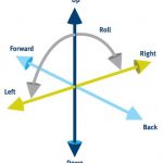
Imagine that all OEM uses the same GPU (integrated as an IP core into the Application Processor), then how will they differentiate? CEVA, the DSP IP core leader supplier, has developed a very interesting piece of S/W, the digital video stabilizer (DVS) software module for the CEVA-MM3000 imaging and vision platforms,bringing advanced imaging capabilities to next generation smartphones and mobile devices. Just take a look at the above picture, you can see various axis, linked to all the motion that any human being can do, even when he is trying to take a picture. Which is a problem in this case, as you would like this human being to stay absolutely unmoving. Unfortunately, this is not possible! Using CEVA DVS will allow correcting this behavior, it will also allow the OEM to differentiate, as DVS function is adaptable and allow various calibrations. You can see the main features of CEVA DVS, 4-axis motion correction, Rolling Shutter correction and scalability on the picture below:

The problem with previously designed DVS functions was the associated power consumption, estimated to be in the range of 1 Watt by CEVA. The company claim 35 mW power consumption associated with the DVS used with MM3000 imaging and vision DSP platform! If you want to check for the effectiveness of CEVA DVS, just take a look at the picture below, showing a comparison with Apple iPhone 5, HTC One X or Samsung Galaxy Note 2. Going to the YouTube link http://youtu.be/7YmXJLe_CZo will give you a better idea of the DVS quality.

Talking about DVS, it can be interesting to explore how it works. DVS is using various pre-optimized kernels:

  • Harris Corner/”GoodFeaturesToTrack”

    • Detecting features for tracking
  • KLT

    • Tracking the Optical features using optical flow
  • RANSAC

    • Estimating the camera motion model
  • Kalman

    • Smoothing the camera motion
  • Affine Transform

    • Correcting the distortions generated from the motion and rolling shutter

DVS also using automated frame management mechanisms. Once again, the important point is that an OEM can integrate in the Application Processor a CPU core (or should I say an ARM set of cores?), an internally designed (or externally sourced) GPU and MM3000 imaging platform and differentiate by using this programmable DVS, allowing an extremely low power consumption: 35 mW for a 1080p and 30 fps when implemented in 28nm. Every OEM wants to differentiate through the GPU? Every OEM can differentiate even more by using DVS and MM3000 from CEVA in conjunction with homemade GPU!

A company like CEVA enjoys more than 200 licensees and 300 licensing agreements signed to date, CEVA’s comprehensive customer base includes most of the world’s leading semiconductor and consumer electronics companies. Broadcom, Icom, Intel, Intersil, Marvell, Mediatek, Mindspeed, Mstar, NEC, NXP, PMC-Sierra, Renesas, Samsung, Sharp, Solomon Systech, Sony, Spreadtrum, ST-Ericsson, Sunplus, Toshiba and VIA Telecom all leverage CEVA’s industry-leading platform solutions and DSP cores.

Eric Esteve from IPNEST

lang: en_US


No Mention of 14nm at the 2013 Intel Developer Forum?

No Mention of 14nm at the 2013 Intel Developer Forum?
by Daniel Nenni on 08-19-2013 at 5:00 pm

Yes, I will be going to IDF again this year, even though it is the same day as the Apple new product announcement. As a born again Apple Fan that is really saying something but Intel has done a great job of motivating the fabless semiconductor ecosystem and I thank them for that.

Unfortunately, noticeably missing from the IDF presentation line-up is 14nm. The semiconductor equipment people continue to tell me that the 14nm move-in has been delayed a quarter or two. I will be investigating this further at IDF for sure, mostly at the 150+ company technology showcase since Intel does not control that information flow.

Also missing from the IDF technical line up are smartphone sessions. Tablets yes but smartphones no, which is telling. As I have mentioned before, making an SoC is a completely different thing than making microprocessors, which is why there has been a 12 month Atom lag in the past. If Intel is to have any chance in mobile that must change and I’m hoping to hear as much at IDF. No mention of Intel TV and wearable devices either. Intel missed the mobile high margin days so let’s hope they make it in time for TV and watches.

The keynotes are very much mobile though:

IDF 2013 represents the beginning of a new era for Intel, and indeed the entire computing industry. With the recent leadership transition now complete, Intel’s new CEO Brian Krzanich and President Renée James are well underway in resetting the course of the company with a clear emphasis on mobile computing leadership. Please join Brian and Renée to hear how this focus on all things mobile will energize the existing ecosystem of Intel hardware and software developers – as well as attract a new wave of developers. There has never been a better time to align with Intel as a company and on the most scalable, widely deployed and successful architecture of all time.

Tuesday, September 10 Mobilizing Intel
Brian Krzanich, Intel CEO, Renee James, Intel President

Wednesday, September 11 Innovate at the Speed of Mobility
Douglas Fisher, Vice President, General Manager, Software and Services Group
Kirk Skaugen, Senior Vice President, General Manager, PC Client Group
Dr. Hermann Eul, Vice President, General Manager, Mobile and Communications Group

Thursday, September 12 Seven billion futures, and you’re one of them
Dr. Genevieve Bell, Intel Fellow, Intel Labs, Director, Interaction and Experience Research

You can get the full IDF 2013 agenda HERE. IDF has been around since 1997 and is a staple technical conference for the PC industry. It will be interesting to see how many familiar faces I see this year as Intel penetrates the fabless semiconductor ecosystem through the foundry business. Last year I saw not one fabless person that I recognized, except for Paul McLellan. Nobody recognized me either, not one autograph or even a nasty look from one of the many Intel shills. This year should be different, absolutely!

Why am I so hard on Intel? Because I think technology monopolies are bad, they stifle innovation and seek to control markets that should not be controlled. It’s a Star Wars thing, may the force be with us!

Also Read: Intel Really is Delaying 14nm….

lang: en_US


More to the story than bigger FPGA-based prototyping

More to the story than bigger FPGA-based prototyping
by Don Dingee on 08-19-2013 at 5:00 pm

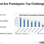
Still not convinced on the value of FPGA-based prototyping systems, or using older technology? I’ve been trying to find the story beyond just bigger, badder FPGAs in a box that you pour RTL into – and found some hints in a webinar on the Synopsys HAPS-70 from earlier this year.

Continue reading “More to the story than bigger FPGA-based prototyping”


Atrenta Seminars in Asia – Making RTL Signoff Real

Atrenta Seminars in Asia – Making RTL Signoff Real
by Daniel Nenni on 08-18-2013 at 8:10 pm

Engaging with the semiconductor ecosystem is critical to surviving in the fast paced times we work in. Face to face interaction at all levels is key and semiconductor IP is a prime example. How do you ensure that your IP meets objective quality requirements before integration into your SoC, and that your SoC is ready for handoff to the back-end implementation?

RTL Signoff is here. A growing number of design teams rely on Atrenta’s RTL platform to certify their IP choices and ensure their designs are implementation ready. Adding a signoff flow at RTL provides them a competitive edge that can mean the difference between success and failure.


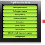
Atrenta’s SpyGlass Predictive Analyzer® significantly improves design efficiency for the world’s leading semiconductor and consumer electronics companies. Patented solutions provide early design insight into the demanding performance, power and area requirements of the complex system on chips (SoCs) fueling today’s consumer electronics revolution. More than two hundred companies and thousands of design engineers worldwide rely on SpyGlass to reduce risk and cost before traditional EDA tools are deployed. And with the addition of BugScope™ verification efficiency is also enhanced, allowing engineers and managers to find the fastest and least expensive path to silicon for complex SoCs.

Join us for a live seminar to learn more about RTL Signoff:[TABLE] cellspacing=”3″ style=”width: 410px”
|-
| style=”width: 50px” | 9:30 AM

| style=”width: 207px” | Arrivals & check-in

|-
| 9:50 AM
| Introduction of speakers
|-
| 10:00 AM
| Introduction to Atrenta, RTL Signoff and IP Kit
|-
| 10:45 AM
| How to get signoff confidence for CDC
|-
| 11:30 AM
| Verification signoff – using assertion synthesis
|-
| 12:15 PM
| Lunch & networking
|-
| 1:30 PM
| RTL power reduction and power signoff
|-
| 2:15 PM
| Timing is everything – getting constraints right
|-
| 3:00 PM
| Break
|-
| 3:15 PM
| How to simplify RTL restructuring
|-
| 4:00 PM
| Achieving quality goals – DFT at RTL
|-
| 4:45 PM
| Lucky draw & event conclusion
|-

Register todayas seating is limited for this FREE event:

[TABLE] style=”width: 400px”
|-
| style=”width: 200px” | Beijing, China
Sep 23, 2013
| width=”200″ |
|-
| style=”white-space: nowrap; vertical-align: top” |
| style=”white-space: nowrap; vertical-align: top” |
|-
| style=”white-space: nowrap; vertical-align: top” | Shanghai, China
Sep 25, 2013
|
|-
| style=”white-space: nowrap; vertical-align: top” |
| style=”white-space: nowrap; vertical-align: top” |
|-
| style=”white-space: nowrap; vertical-align: top” | Hsinchu, Taiwan
Sep 27, 2013
|
|-
|
|
|-
| Seoul, South Korea
Oct 02, 2013
|
|-

Register todayas seating is limited for this FREE event:

lang: en_US


Hogan’s Labor Day Luau

Hogan’s Labor Day Luau
by Paul McLellan on 08-16-2013 at 11:57 am

Jim Hogan is having his annual Heart of Technology charity barbecue at his home in Santa Cruz. This year it is on Saturday August 31st and it’s a luau. It is from 2pm to 8pm at 2171 Sunny Acres Drive, Santa Cruz. Each adult requires a tax-deductible donation of $50 to FleaHab of Santa Cruz County (kids are free).

In addition to Hawaiian food, there will be dozens of auctions of products from local businesses and artisans including a 1938 old-growth redwood and balsa surfboard and one-of-a-kind bronze sculpture by noted local artist David Kimball Anderson, resort stays, wine, massages, jewelry, and much more in both live and silent auctions.

FleaHab was founded in 2011 by surf legend Darryl “Flea” Virostko and integrates exercise and a healthy lifestyle into the recovery process for those afflicted with drug or alcohol addiction.

This is the social event of the summer for anyone in EDA, semiconductor, the investment community and more. Don’t miss it.

For more details and to buy tickets go here.


Why Adopt Hierarchical Test for SoC Designs

Why Adopt Hierarchical Test for SoC Designs
by Daniel Payne on 08-15-2013 at 4:37 pm

IC designers have been creating with hierarchy for years to better manage large design sizes, however for the test world the concept of hierarchy and emerging standards is a bit newer. TSMC and Synopsys jointly created a webinarthat addresses hierarchical test, so I’ve attended it this week and summarized my findings here.Adam Cron, Synopsys Continue reading “Why Adopt Hierarchical Test for SoC Designs”


Funding Startups the SK Telecom Way

Funding Startups the SK Telecom Way
by Paul McLellan on 08-15-2013 at 4:15 pm

At the recent GSA Entrepreneurship Forumone of the panelists was Angel Orrantia of Innopartners who are trying a novel approach to funding startups in the semiconductor space and the surrounding ecosystem.

It seems things got started with an innovation center inside SK Hynix. Just in case you have forgotten, Hynix is the newish name for Hyundai Electronics (the name comes from HYundai electroNICS) which subsequently merged with LG Semiconductor. In 2012 SK group acquired a 21% share of Hynix. The corporate structure is complex, but the important bits are that SK Telecom is the parent of SK Hynix and of SK Telecom Americas inside which is the Innopartners Innovation Center where Angel works. Phew.

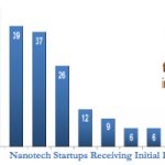
SK had historically grown by identifying and acquiring companies (like, well, Hynix) but it was getting historically hard to find companies to build the portfolio since the innovation model of venture capital funding was broken in this area. VCs only want to invest in companies that have a chance of being the next Instagram or Dropbox. For instance, in 2003 there were 44 semiconductor/nanotechnology companies funded; in 2011 just 3.

So if there are no companies to harvest then it is time to create your own garden and grow some yourself.

So in April this year Innopartners was founded here in Silicon Valley (in Sunnyvale in temporary quarters while the building they will eventually occupy is being built). They have been actively looking for investments for a few months and close to closing the first few (two expected by the end of August, 3-5 by the end of the year).

The investment model is to bring companies into the incubator for 6-12 months, although there is no fixed timetable. That gets them through to the seed stage where a prototype exists, or some data is validated. They then look for strategic investors. Strategic is a sort of code word in the investment world meaning companies that are not just financial: they are at least potentially interested in the technology for use internally. SK also have SKTA which can invest along with strategic (and even VCs if there are any interested) for a 2-3 year funding horizon.


The intention is that eventually the company will be acquired by a strategic partner. This could be SK Telecom or Hynix but there is no obligation to feed all investments back inside in that way, it depends on who the most appropriate partner is. For example, a materials company might find a home in a semiconductor equipment company. Since Hynix builds semiconductors, of course, it might still benefit strategically from the investment even without acquiring it. Or, like so many startups, the precise business might have morphed into something else and no longer be as good a match.

The SK Innopartners white paper is here.


Accelerating SoC Simulation Times

Accelerating SoC Simulation Times
by Daniel Payne on 08-15-2013 at 2:43 pm

There never seems to be enough time in a SoC project to simulate all of the cycles and tests that you want to run, so any technique to accelerate each run is welcomed. You can just wait for your software-based RTL simulator to finish running, or you can consider using a hardware-based accelerator approach. I learned more about one such acceleration approach from Aldec at a recent webinar entitled, Accelerate SoC Simulation Time of Newer Generation FPGAs.


Bill Tomas, Aldec

Continue reading “Accelerating SoC Simulation Times”