llmda newsletter ad (2)

The TSMC OIP Technical Paper Abstracts are up!

The TSMC OIP Technical Paper Abstracts are up!
by Daniel Nenni on 08-25-2013 at 8:10 pm

The TSMC Open Innovation Platform® (OIP) Ecosystem Forum brings TSMC’s design ecosystem member companies together to share with our customers real-case solutions for customers’ design challenges and success stories of best practice in TSMC’s design ecosystem.

More than 90% of the attendees last year said “this forum helped them better understand the components of TSMC’s Open Innovation Platform” and “they found it effective to hear directly from TSMC OIP member companies.”

This year, the forum will feature a day-long conference starting with executive keynotes from TSMCin the morning plenary session to outline future design challenges and roadmaps, as well as discuss a recent collaboration announcement, 30 selected technical papersfrom TSMC’s EDA, IP, Design Center Alliance and Value Chain Aggregator member companies, and an Ecosystem Pavilion featuring up to 80 member companies showcasing their products and services.

Date: Tuesday, October 1st, 2013

Place: San Jose Convention Center

Attendees will learn about:

  • Design challenges in 16nm FinFET, 20nm, and 28nm
  • Successful, real-life applications of design technologies and IP
  • Ecosystem specific implementations in TSMC reference flows
  • New innovations for next generation product designs

In addition, attendees will hear directly from our design ecosystem member companies talk exclusively about design solutions using TSMC technologies, and enjoy valuable opportunities for peer networking with near 1,000 of industry experts and end users.

TSMC Open Innovation Platform Ecosystem Forum is an “invitation-only” event: : please register in order to attend. We look forward to seeing you at the 2013 Open Innovation Platform Ecosystem Forum.

Registration: Join the TSMC 2013 Open Innovation Platform® (OIP) Ecosystem Forum to be held on Tuesday, October 1st at the San Jose (CA) Convention Center.

Established in 1987, TSMC is the world’s first dedicated semiconductor foundry. As the founder and a leader of the Dedicated IC Foundry segment, TSMC has built its reputation by offering advanced and “More-than-Moore” wafer production processes and unparalleled manufacturing efficiency. From its inception, TSMC has consistently offered the foundry segment’s leading technologies and TSMC COMPATIBLE® design services.

TSMC has consistently experienced strong growth by building solid partnerships with its customers, large and small. IC suppliers from around the world trust TSMC with their manufacturing needs, thanks to its unique integration of cutting-edge process technologies, pioneering design services, manufacturing productivity and product quality.

The company’s total managed capacity reached 15.1 million eight-inch equivalent wafers in 2012. TSMC operates three advanced 12-inch wafer fabs, four eight-inch wafer fabs, and one six-inch wafer fab in Taiwan. TSMC also manages two eight-inch fabs at wholly owned subsidiaries: WaferTech in the United States and TSMC China Company Limited. TSMC also obtains eight-inch wafer capacity from other companies in which the Company has an equity interest.

lang: en_US


Intel Really is Delaying 14nm Move-in. 450mm is Slipping Too. EUV, who knows?

Intel Really is Delaying 14nm Move-in. 450mm is Slipping Too. EUV, who knows?
by Paul McLellan on 08-24-2013 at 3:23 pm

I attended the semi-annual SEMI Silicon Valley Lunch meeting last week. The semiconductor equipment people are the ones that really know what is going on. People can talk about capex numbers on conference calls but it is the equipment vendors who either do or do not get orders for particular types of equipment. In turn, the analysts that follow the equipment industry have a pretty good handle on where various technologies are.

Also read: Intel 14nm Delayed?

One takeaway was that Intel’s delay of a quarter or two in 14nm was just taken as a given during the lunch. Intel has the biggest capex in the industry (although actually TSMC spent more in the first half of the year) so changes in their spend affect everyone. Intel has reduced its expected capex for the year to $10B but the analysts were skeptical that they would be able to spend that much given that there are only 4 months left in the year.


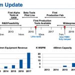
Another area of contention was 450mm wafers. Gartner has Intel and TSMC fully-ramped onto 450mm by mid-2018 but IC Insights have it a year later in 2019. Partly this is because of the uncertainty of when (or even if) EUV will be available. 450mm has a bigger saving of around 30% if there is no need for lots of double patterning. So it seems that maybe in 2015-16 there will be some 10K WPM pilot lines with full production in 2019.

One big uncertainty is what comes after DRAM. Everyone has forecast the end of DRAM many times before, of course, but at some point the capacitor really will stop scaling. Memristor-based memories could be the next thing but there seems to be a requirement for EUV to be able to manufacture them.


IC Insights had third quarter forecast for the industry. Intel at #1 with $12.3B followed by Samsung at $8.1B and TSMC at $5.4B. Qualcomm is $4.2B. I asked Brian if they did anything about the double counting for fabless companies: namely, all the silicon Qualcomm ships also shows up in TSMC’s and Global’s numbers too, and he said they did not.


He had another interesting chart: if you value TSMC’s silicon as final sales into the end market (making reasonable assumptions about TSMC’s customers’ margins) then TSMC is bigger than Intel. That is, TSMC and its customers taken as a sort of conglomerate has just passed Intel in revenue.


Another surprising statistic was the strength of the Chinese market. China is now the #1 market for PCs, for automotive, for cell-phones and for digital TV.


And how much will the semiconductor market grow overall in 2013. The answer seems to be 6%. But if you take DRAM out (where pricing has strengthened due to consolidation down to Samsung, Micron/Elpida and SK Hynix) it is just 4%. On the other hand, some of the weakness is due to the Japanese market being valued in yen, and the yen has weakened from roughly 80Y/$ to 100Y/$. If you use last year’s exchange rate then the market grew 8%.


Foundry has been increasing over the years as many IDMs have switched to fab-lite models and as the overspend in the memory markets has been got under control. This year it is expected to be 38% of all capital spending, rising to 41% the year after. I’m not quite sure how Samsung and Intel are counted in this as they are IDMs that also do foundry business.

The slides for the presentations will be on the SEMI websitesoon. There is an issue converting a couple of slides. The page for the lunch with speaker bios etc is here.

UPDATE: the presentations are here.


Low-Power Design Analysis and Optimization for Mobile and High-Performance Computing Applications

Low-Power Design Analysis and Optimization for Mobile and High-Performance Computing Applications
by Daniel Payne on 08-23-2013 at 7:36 pm

For several decades now consumers like me have enjoyed using mobile devices including:

  • Transistor radios, my first one had just 6 discreet transistors in the 1960’s
  • HP 21 Calculator, used in college with Reverse Polish Notation, circa 1976
  • Zenith Data Systems laptop, with two floppy drives, 1980’s
  • Palm Pilot V, a useful PDA before smart phones that is, 1990’s

Fast forward to today where I enjoy using mobile devices with up to billions of transistors:

  • MacBook Pro 17″ with 16GB of RAM, and an Intel Quad Core i7 processor
  • iPad 3 with 16GB of Flash, and A5X quad-core ARM processor
  • Samsung Galaxy Note II with 5.5″ display, powered by a quad-core Cortex-A9 processor


We have grown very accustomed to new generation devices that have faster performance, lower power and run longer on a single battery charge. These three general trends place a daunting challenge on SoC and electronic system designers. Fortunately there is some help in sight by using EDA tools that can:

  • Measure power at the chip, package and board levels at the earliest point in your design process to see if you will meet the target specifications
  • Verify power integrity for sub 1 V supply levels for the many modes of your SoCs
  • Simulate all of your high-speed low-power I/Os, like LPDDRs to verify they work in the presence of core and system noise within your jitter specs
  • Perform checks for Electromigration (EM) and Electrostatic Discharge (ESD) to ensure a long product life
  • Run thermal simulations to see how stable your electronic design really is


Apache Ultra Low Power Flow

There’s a webinar hosted by ANSYS-Apache on Tuesday, August 27th that will address these specific types of analysis, starting at 4PM EDT or 8PM GMT. Registration is required so sign-up here.

You will hear about how to design mobile and high-performance ICs for power and reliability using the simulation platforms engineered by ANSYS-Apache. The webinar will last 60 minutes, is free, and you’ll have a chance to ask questions about how the Apache tools work.

lang: en_US


Microsoft Signals the Return of "Expensive Hardware, Cheap Software"

Microsoft Signals the Return of "Expensive Hardware, Cheap Software"
by Ed McKernan on 08-23-2013 at 12:00 pm

The announcement that Steve Ballmer will step down from Microsoft within the next 12 months and just weeks after kicking off a vast re-org focused on mobile devices can only mean that the future is coming much faster than Bill Gates or Steve Ballmer had ever expected and that without a radical adoption of hardware everywhere, it will leave the company without an existence (sans PC legacy) anywhere. The illness that effects Microsoft and Intel is a back to the future moment as the 30 year PC ecosystem dominance of Wintel will in the years to come likely be viewed as a radical departure from the traditional requirement that hardware and software co-existance is necessary in order to truly dominate. Thus the model of the IBM mainframe, the early Apple Mac and now the iphone/iOS platform shows that one ecosystem eventually dominates every generation, thus garnering more than 60% of the profits. We are way past the tipping point and Microsoft lacks ownership of hardware to drive its way forward. Be prepared for acquisitions such as Nokia as they aim for a comeback.

The mistake that Apple made, following the departure of Steve Jobs after the launch of the MAC was to rest on its high profit laurels. With what turned out to be a 10 year operating system lead, John Sculley had plenty of time to move Apple into a dominant position by building out a mid range and even entry level market in order to pull in the majority of the software world as Win 3.1 from Microsoft didn’t appear until 1992. And let’s not forget Microsoft held the O/S close enough to be the first to release the killer office applications. Only Lotus 1-2-3 and a few antiquated word processing apps gave the impetus for corporations to buy PCs in the 1980s. Think what might have been had Sculley acquired Lotus or incentivized them to come to market with a MAC version of 1-2-3 years before it appeared in 1991. A Mac selling for even $500 more than a PC but pre-installed with 1-2-3 would have driven the platform to dominance through the 1990s by the fact it would have won the highly prized corporate world.

Take note: Hardware Expensive, Software Free = Worldwide Dominance.

Back through history this has played out over and over and is now becoming the law of the land again. In the 1960s and 1970s, IBM sold expensive hardware with a bevy of free software and also expensive maintenance contracts. It would have carried over in the PC era if they had control of the hardware and the O/S. That minor detail shifted the profits to Intel and Microsoft or “Wintel.” However, Microsoft had the true upper hand as PC costs dropped by an order of magnitude from the original $5000 sticker price in 1981 until the beginning of this decade while they served up to corporate what it wanted most: the high priced “Office” productivity apps.

The latest earnings announcement from HP, which now has had its gross margins reduced to roughly 20%, is a sign that for even legacy to continue, Microsoft will have to take over the hardware business in order to guarantee that the razors get into the actual hands of users. Otherwise the razorblades sit on the shelf like outdated bananas. Intel is in a similar quandary on the client side and will ally themselves to the volume mobile manufacturers in order to guarantee volume for the fabs. Their true hope is that the rise of mobiles pushes more of the heavy lifting to the cloud where Xeon servers sell at a premium. Does Intel cheap mobile + expensive cloud servers mean increased revenue and profits? TBD

This past year and the coming months will truly test whether we are returning to an era of “expensive hardware and cheap software.” Apple has been severely tested by a mobile world inundated with cheap Android phones, some selling down to below $70. The market has shown over the past year that there is first and foremost a huge demand to move from feature phones to “internet phones.” Secondly, Apple has shown in test markets like India and the USA that when it moves the iphone into a midrange price point, the demand increases substantially. In addition it has increased its market share in enterprise to over 60% – does that number ring a bell?

Apple is at that 1985 moment again when Sculley decided to go for profits instead of following the Steve Jobs plan of figuring out how to sell a MAC to the masses and thereby capturing the dominant ecosystem position. Steve Jobs had wanted to price the original MAC down at $1000, however the hardware horsepower necessary to run the Operating System was more costly than first expected. Jobs knew however that Moore’s Law would be able to get him there within a couple turns of the crank and with the right roadmap they could have hustled to get there in the late 1980s.

If Apple is able to successfully lock down the midrange market with its new iPhone 5C, reportedly to be introduced on September 10[SUP]th[/SUP], than I expect that they will win the compute ecosystem of this generation. The cheap hardware, expensive software of the PC generation transitions to the “expensive hardware and cheap software” of the mobile generation. The ecosystem win will be underwritten by the corporate world, which demands standards and security and not by the worldwide masses of new mobile users who first enter at the thin margins.

lang: en_US


20nm IC production needs more than a ready Foundry

20nm IC production needs more than a ready Foundry
by Pawan Fangaria on 08-23-2013 at 11:00 am

I think by now all of us know, or have heard about 20nm process node, its PPA (Power, Performance, Area) advantages and challenges (complexity of high design size and density, heterogeneity, variability, stress, lithography complexities, LDEs and so on). I’m not going to get into the details of these challenges, but will ponder on the flows and methods which can overcome these and can generally be available for a larger design community for mass production of ICs at 20nm; of course, based on the rules and regulations laid down by foundries. If anyone wants to refer to details of these challenges, she/he can refer to an earlier paper published by Cadencehere.

Sometime in Jun/July this year, it was reported by TSMCthat their risk production of 20nm chips has already started and volume production will start by Dec this year or early next year. It is known that Apple(for its A8 processors), its first customer is already lined up, more may join the queue. It must be noted that in last quarter of 2012 TSMC also announced support of double patterning technology and multi-die integration and corresponding reference flows for 20nm process node.

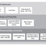
For proliferation of this technology into mass production by leveraging the sea of design houses, EDA vendors must provide the complete holistic solutions to overcome these challenges rather than point tools. At 20nm, that need becomes more prominent because it changes the paradigm in the context of double patterning complexities, variability and interdependence between design phases and manufacturing. The designers can no longer wait to fix problems until layout sign-off, everything has to be done in parallel at each stage.


[Challenges and requirements for 20nm IC design]

As we see, tackling these issues in the design is not enough, the design closer needs to happen in time and with desired PPA in order to avail the window of opportunity in the market. Having earlier worked at Cadence, I can firmly say that this is one company which provides a complete end-to-end solution to the overall design flow, with the whole spectrum of EDA tools for all types of designs; custom, digital, mixed-signal and so on. This company has the right expertise, through its long tenure in semiconductor EDA domain, to address designers’ need at all levels. For example, analog design needs more customized approach whereas digital design has very high level of automation.


[Cadence GigaFlex technology – A flexible modelling approach to manage large designs]

Cadence proposes rapid prototyping and rapid verification methodologies to save significant amount of design time. It uses flexible modelling to support required level of abstraction at each stage. For example, the model at design exploration or planning stage does not require details of that used at block implementation level. Further, it uses an innovative “Prevent, Analyze and Optimize” approach which drives both custom and digital platforms to enable faster design convergence at advanced nodes. In-design sign-off is done at each stage such as placement, routing, lithography analysis, timing and signal integrity and so on by utilizing state-of-the-art sign-off quality tool engines. Also correct-by-construction approach is used at the design time by utilizing smart tools such as constraint-driven design, LDE-aware placement, color-aware P&R and in-design verification.


[Clock Concurrent Optimization combines timing-driven CTS with physical optimization]

Clock Concurrent Design Flow is a paradigm shift that makes Clock Tree Synthesis (CTS) timing window-driven rather than skew-driven, and merges it with physical optimization. This provides significant PPA optimization; 30% saving on power and area and 100MHz of chip performance improvement for a GHz design with ARM processors.

To conclude, there are several challenges to fetch the benefits of 20nm technology, but with right tools, methodologies and collaboration across semiconductor ecosystem, they can easily be achieved. There is a detailed whitepaper from Cadence on the methodologies to be used for 20nm designs, “A Call to Action: How 20nm will Change IC Design”. It’s worth looking at, I enjoyed reading it and jotted down a summary of that in this article. The paper also has other references on 20nm technology. Enjoy reading!!


NoC adoption surge at Chinese chip maker

NoC adoption surge at Chinese chip maker
by Eric Esteve on 08-23-2013 at 9:55 am

The news from Arteris, Inc., announcing that “its interconnect fabric IP has been licensed and deployed in a majority of chips developed by China’s leading semiconductor companies for applications including consumer electronics, smartphones, and tablets,” is holding attention for several reasons. At first, because it’s a clear indication that the Network-on-Chip (NoC) has become an indispensable piece to design a System-on-Chip (SoC), although the commercial NoC is less than ten years old. The second point is that this news highlight Arteris supremacy on the interconnect fabric IP (the other NoC name), despite the desperate effort from one of Arteris competitor to limit this success story, even by using legal battle field instead of trying to develop a better competitive product. We, at Semiwiki, have already blogged several times about the NoC features and the benefits it bring when implemented into a SoC, like to reduce wire congestion and ease intra-chip communication. We also blog about this legal battle, and we have clearly expressed our opinion: trying to compensate a lack of innovation by going to the legal field without good reasons is…#%¤!!&, and even more!

Let’s concentrate on the fact that four of the top five Chinese chip maker addressing consumer, wireless and tablet market segment have integrated a commercial NoC. I remember from discussion I had with Kurt Schuler, VP of Marketing with Arteris, that he told me about the early phase of business development, when Arteris sales force was trying to design-in the NoC five or six years ago to the large SoC chip makers in Europe and USA: at that time, the real competition was with the internally designed solution. Everybody who has ever to fight with the NIH syndrome knows that it is even more difficult to displace an internal design. Quite often, you try to sell a product to the same people who have developed an identical solution, explaining that your product is better, so they just fell stupid. They know that, if you are successful, they may lose their jobs, or at least their credibility… not an easy story.

Which is remarkable with Chinese chip makers is how fast they came up to speed, competing with, by far, older companies able to capitalize on long established R&D teams and associated know-how. These start-ups had to move quickly, so they faster took the right decision: integrate an off-the-shelf product, validated in dozen of SoC design – and in production on billions of IC (we are talking about the consumer and wireless market). This remind me the emergence of GSM based cell phone in Scandinavia. Did you ever ask yourself why the very first GSM cell phone successful manufacturers were Ericsson (Sweden) and Nokia (Finland)? Just because during the long winter the earth is frozen, so implementing a wired phone network is very painful! Developing an Application Processor and managing the intra-chip communication is certainly a great challenge when you start from scratch, a good way to minimize this challenge is simply to implement a commercial NoC!

If you listen to Analyst, they say it differently, but the idea is the same: “We see a very dynamic market in China’s local integrated-circuit (IC) design market, with double digit year-over-year growth projected for 2013,” said Vincent Gu, Principal Analyst, Market Intelligence, with IHS iSuppli. Tools such as Arteris’ network-on-chip interconnect IP fabric enable these design firms to more effectively meet the growing demand for semiconductors in China at a lower cost point.” Based on the IHS iSuppli ranking of the top Chinese fabless semiconductor OEMs in terms of revenue, Arteris counts four of the top five OEMs as customers – Spreadtrum Communications, HiSilicon Technologies, RDA Technologies and Allwinner Technology. Just listen to Arteris’ customer feedback:

“Arteris has provided exceptional support to our teams, giving us the confidence to implement the FlexNoC solution in our critical Smartphone SoC platform,” said Li Shiqin, IC Design Manager at Rockchip.

“The Arteris FlexNoC commercial SoC interconnect fabric IP gives us the performance required by our customers,” said Ding Ran, chief technology officer of Allwinner Technology. “We have seen first-hand how the interconnect IP improves process flow and overall system performance.”

Let say that I completely agree with Charles Janac, saying: “Arteris has achieved significant market share in the China fabless semiconductor market by not only solving our customers’ design challenges, but also by enabling them to quickly adopt best-of-breed technologies and development practices,” said K. Charles Janac, President and CEO of Arteris. “The Arteris interconnect IP fabric technology is one of the most significant SoC cost reduction and productivity innovations of the current decade, based on technology results and market adoption.”

Eric Esteve from IPNEST


Jasper: Negronis on tap

Jasper: Negronis on tap
by Paul McLellan on 08-22-2013 at 6:26 pm

Did you know that Jasper’s Corner Tap in San Francisco serves Negronis on tap? It’s true. They also have Hanky Panky on tap, which is a Negroni with the Campari replaced with Fernet (which everyone pronounces as Frenet despite it being…well…wrong). And here’s another thing you probably didn’t know: San Francisco itself accounts for over 25% of all US consumption of Fernet. My daughter is a bar manager, I learn all kinds of stuff.

Anyway, talking of Jasper (this has to be the worst segue I’ve ever written) I doubt that there will be Negronis on tap at the Jasper User Group meeting but I’m sure that they will have free beer and wine as usual at the cocktail reception on October 22nd. The Jasper User Group (JUG) will be on October 22nd and 23rd. So those will be JUG wines then. It will be in the Cypress Hotel in Cupertino where it has been for the last few years.

I can’t tell you who the keynote is going to be yet because it hasn’t finally been confirmed, but last year it was Intel. Yes, that would be the same Intel that never endorses EDA companies in any way shape or form. If you missed my blog on the history of formal verification at Intel last year then it is still around.

But one of the other presenters could be you. Well, you have to be a Jasper user, of course (or maybe from Intel) but as in previous years, JUG will consist mainly of Jasper’s customers talking about their own experiences rather than a lot of Jasper marketing Powerpoint. Presentations can be from 30 minutes to an hour long.

Topics of interest include:

  • designer-based verification
  • low-power verification
  • security
  • sequential equivalence checking
  • architecture validation
  • SoC integration
  • RTL development
  • property synthesis
  • post-silicon debug
  • verification IP
  • formal property verification

If you are interested in presenting, then contact Rob van Blommestein robvb@jasper-da.com. Proposals are due by September 21st and then the final presentations by October 18th.

New this year there are “birds of a feather” discussions during breakfast hosted by power users at 8.30-9.30am each morning. Session topics are:

  • proof grid
  • property synthesis
  • clock and reset setup and verification
  • IP-XACT
  • low power verification
  • AMBA Proofkit certification
  • Protocol verification
  • security path verification

Details on those Jasper Negronis here. More details about the Jasper User Group are here. Register for the Jasper User Group here.


Innovation + Thoughtful Management = Productive Expansion

Innovation + Thoughtful Management = Productive Expansion
by Pawan Fangaria on 08-22-2013 at 12:00 pm

After looking at various aspects of this company, to sum up, I couldn’t find any better statement than this; thoughtful management here is actually leadership with passion which achieves tangible results. This reflects in the methodology of doing things in this company which has given it a place among top EDA companies in a span of 12+ years; amid so many macroeconomic uncertainties during that time. Of course, the CEO and the top management of the company have spent many more years in this industry and are well known. You must have guessed it right from the picture; I am talking about Atrenta, or better I should say, SPYGLASS!


[Dr. Ajoy K. Bose along with Sushil Gupta and his staff at the Ribbon cutting ceremony at Atrenta, Noida]

On this Monday, 19[SUP]th[/SUP] Aug, I attended the inauguration ceremony of Atrenta’s expanded new facility at Noida and had an opportunity to talk to Dr. Ajoy K. Bose, CEO of Atrenta. Seeing Atrenta’s success in the SoC Realization arena, I had certain queries, or rather some assumptions in my mind; those were cleared during my talk with Ajoy. From this conversation, one can easily make out that the above statement holds true.


[Sushil Gupta, V.P. and MD at Atrenta, Noida lighting the auspicious lamp]

The Conversation –

Q: Your Noida centre has grown to about 200 people, the largest R&D centre in this beautiful, world-class, spacious facility. Of course there would be several reasons to invest in Noida, but tell me one prominent, compelling reason to invest in India, Noida.

This goes back to my initial days in early 1990 when I Joined Cadence and got involved with their India operation which had about 20 people at that time. It was then that I learned about power of Indian engineering. We had a shortage of talent in EDA R&D at that time, and we found that the kind of expertise and competence Indian engineers possessed, their attitude, willingness to learn and do, software development skills, process adherence, quality consciousness etc. were the right fit for us. And that is continuing today. Now the second part – why Noida? That is because of grooming of people around this region into our domain since then and availability of fresh talent.


[Ajoy addressing the staff at a communications meeting]

Q: What are your major product developments in Noida?

At Noida we have our largest development centre; we have almost all of our products being developed here except a few. We have a team in Grenoble, France; they are experts in formal verification and power. Last year we acquired NextOp and they brought us a team in Shanghai that created an assertion-based verification solution. Recently, we have set up a team in Colombo, Sri Lanka too.

Q: Yes, I’d heard about your Sri Lanka initiative. That’s leading by example; I guess no other EDA company is there in Sri Lanka. So, what made you think of Sri Lanka?

There are couple of aspects – I knew some of the best brains and enthusiastic people from Sri Lanka in my career, those people were influencers. Then, the undergraduate courses in universities there are very strong in science and mathematics and the skills required in our kind of industry. And then, proximity of Sri Lanka with India, that plays a vital role in working of the two teams together; the two cultures also assimilate easily.

Q: Now coming towards business side; I see that there are about 350 employees and 200+ customers at Atrenta. So, I guess the employee to customer ratio is quite low?

Yes, but it should not be looked at from that ratio perspective. We have a sufficient number of people to serve our customers well. Field AEs are available where required. The number depends upon the nature of the product. For example, the RTL physical product requires more AEs than we do in other SpyGlass products. And then it depends on size of the business, and the state of maturity of the product too. It’s a time varying phenomenon; we have a flexible organization which is optimized as required.

Q: My other query is related to employees; I see that 75% of work population is in R&D. How do you compare this with the rest of the industry?

Yes, we are high on R&D. We invest in developing new products. We have about 10 products developed in-house and we have been successful in doing that.

Q: So, how do you see the revenue per employee?

We are quite profitable there; R&D costs are very much optimized. We are flexible here. Mature products need less new R&D while new product development requires more initial investment.

Q: That’s quite impressive business leadership. On the technical side, I see that your organization has 49 patents (23 granted, 26 pending). Are all of these productized well? What is the average lead time?

Yes, we have all of these innovations integrated into products; we consciously invest in that. Often, it takes about a year or even two to conceptualize an idea along with some partner customers and then the usual product life cycle takes place. So, it takes about 4 to 5 years to make a full-blown product.

Q: I see that your concentration is on SoC Realization at the RTL level. There are other companies also offering products in that space. So, what is your POD (Point of Differentiation)?

We provide the most complete coverage at the RTL level. These are not used as point tools, although they are best-in-class in their capabilities. We provide a complete solution; SPYGLASS is a complete sign-off platform at the RTL level.

Q: Considering the overall flow from RTL to GDS, are you also focusing on POP (Point of Parity)?

There we cover all aspects of the complete flow, from micro architecture creation to modelling the physical implementation, but we abstract all that to the RTL level. Our theme is to complete the major job at the RTL level and hence save cost in detailed chip design and manufacturing.

Q: SPYGLASS is one of the top EDA products. You must be putting conscious effort towards branding it?

Yes, in DAC 2012 we initiated a major promotion of this brand and the effort is continuing. People know us more by SPYGLASS than Atrenta!

This was a very nice conversation with Ajoy. To conclude on my views, I believe that this company has all that is needed by a top class, productively expanding company. That is, a strong and flexible organization, business leadership, technology leadership and IP leadership. With presence in 11 countries across the world, Atrenta is the largest privately held EDA Company.



Web-based Circuit Design and Analysis

Web-based Circuit Design and Analysis
by Daniel Payne on 08-21-2013 at 11:27 am

Last month I blogged about CircuitLaband received some two dozen comments, so clearly there is keen interest in using web-based tools for electronic circuit design and using the cloud to save designs plus run simulations. Today I’m reporting on TINACloud, provided by a company called DesignSoft.
Continue reading “Web-based Circuit Design and Analysis”


Who is One Step Above Colgate and One Below P&G?

Who is One Step Above Colgate and One Below P&G?
by Paul McLellan on 08-21-2013 at 1:13 am

So who do you think is #31 on the list on Forbes list of the most innovative companies in the world? One place above Colgate and one place below Procter and Gamble. Your first thought is probably why am I asking this on a blog covering semiconductors and going on about toothpaste manufacturers. The answer is Dassault Systèmes. Perhaps more to the point they are listed at #3 in the software and programming category, and #10 amongst European companies.


There are not many companies in the semiconductor ecosystem on the list. I don’t know how the entries are handled but the level of innovation required in EDA, IP, foundry and fabless is unbelievable. I think some of the smaller companies get caught by the minimum market cap of $10B. ARM comes in at #5 on the list, and ASML at #77, two places above Apple (and two behind LVMH Moet Hennessy Louis Vuitton, this list makes for strange bedfellows). Just scraping onto the list at #99 is Mediatek. And if you are interested, Salesforce is #1. The complete list is here. It will be also published in the September 2nd edition on dead trees.

Dassault increased sales by 5% last year, a 5-year total return of 16.7% and the mysterious “innovation premium” of 35.5. The innovation premium is a measure of how much investors have bid up the stock price of a company above the value of its existing business based on expectations of future innovative results (new products, services and markets). In addition to a minimum market cap of $10B, members of the list must spend at least 2.5% of revenue on R&D and have seven years of public data.

As Forbes says:Most innovation rankings are popularity contests based on past performance or editorial whims. We set out to create something very different with the World’s Most Innovative Companies list, using the wisdom of the crowd. Our method relies on investors’ ability to identify firms they expect to be innovative now and in the future. Companies are ranked by their innovation premium: the difference between their market capitalization and a net present value of cash flows from existing businesses (based on a proprietary formula from HOLT/Credit Suisse). The difference between them is the bonus given by equity investors on the educated hunch that the company will continue to come up with profitable new growth.


Dassault were 40th on the list last year, so they have climbed 9 places to 31st this year. In the software area, only Salesforce and VMware are ahead of them. Citrix, Intuit and SAP are the other software companies that are behind them in the top 100 innovative companies.

As of May, when Forbes recorded the data, Dassault had a market cap of $14.22B (today it is close to $17B which probably means their innovation premium has risen too). They have just over 10,000 employees and annual sales of $2.68B. They are the leaders in the 3D design marketplace, the standard for both aerospace and automotive design. With the increasing electronic and semiconductor content they are also moving to start to tie that part of the process in with everything else. It probably hasn’t escaped your notice that both the Airbus 380 and the Boeing 787 had electrical issues.