In case you missed it, there is an interesting conversation on my blog, The Future of Mobile Devices and the Semiconductor Landscape!, between Ashraf Eassa and myself. Ashraf and I also converse privately, he’s a very respectful and intelligent young man. For the last year Ashraf has been writing financial articles for Seeking Alpha which has earned him the reputation of an “Internationally Recognized Intel Fan”.
Ashraf did a nice Intel vs TSMC process comparison in the comment section, clearly he put a lot of time into it and for that I’m grateful. It also gives a telling look into how financial analysts think. Ashraf is a recent college graduate, if you are looking for an entry level analyst make him an offer, absolutely. Unfortunately, Ashraf, along with many other analysts, do not GET the fabless semiconductor ecosystem:
How will the fabless players compete at 20nm if they will not get the performance/power improvements to roughly match Intel’s 22nm FinFET process until 2015 when, presumably, Intel will be shipping its 2nd gen FinFET? Perhaps I’m missing something…
Let’s start at the beginning, the fundamental reason the fabless semiconductor ecosystem exists today is because traditional semiconductor companies did not do their job. They did not have vision, they did not innovate, and most importantly they did not efficiently manage their manufacturing capabilities. The first fabless companies leveraged excess semiconductor manufacturing capacity out of Japan innovating their way into new markets. Chip and Technologies was one of the first and they schooled Intel on how to build PC chipsets. Intel deployed the “if you can’t beat them buy them” strategy and the rest is history. Another early fabless innovator is Xilinx.
It is a familiar Silicon Valley story, Xilinx co-founder Ross Freeman wanted to create a blank semiconductor device that could be quickly programmed based on an application’s requirements. Even back then semiconductors cost millions of dollars to design and manufacture so this was not only a cost savings, FPGAs also dramatically reduced time to market for electronic products. Of course Ross’s employer Zilog did not share this vision and Xilinx was created in 1984. The founder of Zilog was an ex Intel employee who spun out to compete with his employer so he had vision. Unfortunately he had microprocessor blinders on and could not see the big picture. Sound familiar (Intel)?
Fast forward to today, the mobile market owns the semiconductor industry with SoCs driving process technology. The traditional semiconductor companies that once opened up their manufacturing services to the fabless companies are now fab-lite or totally fabless. Intel is also now renting out manufacturing capacity and looks to compete with the top fabless companies for mobile sockets with its Atom processor and superior manufacturing technology. Looks good on PowerPoint, as Ashraf has power pointed out, but the history of the semiconductor industry does not agree.
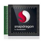
The mobile SoC market is fast moving and Intel is not. Qualcom and Apple alone ship more SoCs than Intel ships processors and at a much lower cost/margin. Qualcomm and Apple both license the ARM architecture and custom tailor their processors to the mobile products they control. Samsung is also licensing the ARM architecture for their line of SoCs. It’s not just a power/performance/price play, it also allows a much higher level of device integration. I don’t EVER see Intel becoming an IP company and licensing the Atom architecture.
The definition of SoC is System on Chip which means all of the semiconductor devices inside your phone will be on one chip at the lowest possible cost/margins. This will require mobile vision, flexibility, and a fast moving product plan. Does that really sound like Intel to you?
lang: en_US