From chip IP vendor ARM Holdings to semiconductor foundry Taiwan Semiconductor, there have been many winners from the mobile device revolution that was sparked by Apple’s introduction of the iPhone. However, while these big-ticket names get all the fame and glory, the electronic design automation space (“EDA” for short) is filled with winners. In short, the EDA companies provide the tools that integrated circuit designers use to actually design and verify their products. In the first part of this three part series on the EDA vendors, I’d like to talk about Synopsys – the leading EDA vendor by revenue.
An Overview
Synopsys was founded in 1986 by David Gregory and Dr. Art J. de Geus (current Chairman and CEO) and a squad of engineers from General Electric’s Microelectronics Center. Since then, through organic growth, a merger with Avanti Corporation, and a broad swath of acquisitions (too many to list!), Synopsys has become the world’s largest EDA tool vendor, with annual revenues just shy of $2B and net income well north of $200M.
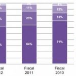
So, what is Synopsys all about, exactly? Well, while I refer to it as an EDA company, a much more appropriate term for it would be an EDA andIP company. Indeed, a look at the breakdown of Synopsys’ revenue base reveals that while EDA tools are the firm’s bread and butter at 62% of revenues during fiscal 2012, the company is growing its manufacturing solution, professional services, and IP and system level solutions businesses at a rapid clip, as shown here:
(Source: Synopsys 2012 Form 10-K)
With this in mind, I’d like to dig into each of these individual product/business segments:
Core EDA
The circuit design process is incredibly sophisticated and consists of a number of rather complex steps from the definition of the architecture to the actual circuit layout. To facilitate this process, Synopsys offers two product lines: the Galaxy Design Platform and the Discovery Verification Platform.
The Galaxy Design platform is a product suite that includes the entire gamut of tools required to design an integrated circuit.
It’s a single, integrated solution that not only comes with a robust set of Synopsys-designed tools, but it also allows chip designers to integrate other third-party as well as home-grown tools. Included in this suite are:
· IC Compiler, which is a tool used for place and route. In IC design parlance, placement refers to the actual placement of the circuitry and logic in a given amount of space. Routing, on the other hand, involves actually “connecting” up all of the different elements per the specification of the manufacturing process (“design rules”).
· Design Compiler ®, a logic synthesis tool. What this does is it takes register transfer level (RTL) description of an IC and cranks out the corresponding logic gates.
· Galaxy Custom Designer, which is a physical design solution for analog/mixed signal designs
· PrimeTime/PrimeTime SI, a suite of products used for timing analysis
In addition to the design tools, Synopsys also provides what it calls the Discovery Verification platform that provides a suite of verification products.
This includes the following tools:
· VCS ®, an RTL verification solution. The term “RTL” (register transfer level) refers to a model of a given IC design in terms of the flow of data between hardware registers and the operations performed on that data
· CustomSim™ FastSPICE which is a circuit simulation/analysis tool
· CustomExplorer™ Ultra, which is a mixed signal regression/analysis tool
· Formality® which is a formal verification sign-off solution
While the percentage of revenues that these tools comprise of Synopsys’ revenue has declined (as its other businesses have ramped), make no mistake – the demand for these tools is quite robust. As the design challenges continue to mount as the industry transitions to FinFETs, the need for more sophisticated EDA tools to get designers through many of the challenges found there is insatiable.
Interestingly, at TSMC’s Open Innovation Platform Ecosystem Forum, TSMC presented a rather interesting chart that showed how far along the three major EDA tool vendors were for developing tools for TSMC’s 16nm FinFET design flow:
Synopsys, as far as TSMC’s FinFET goes, seems to be leading the pack – with Cadence Design Systems a close second and Mentor Graphics in third.
Interestingly enough, on Synopsys’ recent earnings call, CEO Aart J. de Geus notes that 90% of 20nm and below tape outs have used Synopsys, and that the company was already well engaged in 14/16nm FinFETs and even “all the way down to 10-nanometer”. While Mentor and Cadence are certainly formidable competitors that will continue to gain traction as their toolsets gear up for the next generation processes, it looks as though Synopsys continues to maintain its technology lead (no doubt helped by the fact that Synopsys tools were used extensively on Intel’s FinFET chips), as it has already taped out FinFET test chips with Samsung as well as UMC using its tools.
IP and System-Level Solutions
In addition to supplying design and verification tools, Synopsys also is a major player in the semiconductor IP market. Its DesignWare® IP portfolio is loaded to the brim with IP for everything from configurable processor cores, system-on-chip infrastructure IP, interconnect fabric, and various system interfaces such as USB, PCI Express, SATA, and Ethernet. While in the EDA tool space, Synopsys largely competes with Mentor Graphics and Cadence Design Systems, on the IP side of things the company is actually largely competing with firms’ internally designed solutions.
Keep in mind that Synopsys is actually the largest supplier of physical IP – double its nearest competitor. Further, within the top 20 semiconductor vendors, Synopsys’ IP has actually increased fivefold. As far as the overall IP space goes (not just physical IP), Synopsys enjoys a very comfortable #2 position. All told, IP is a double-digit revenue growth business for the company, as it continues to drive leadership in interface, embedded memories, and analog IP (only 50% of the IP blocks in these areas are outsourced, so there’s further room for growth there).
In addition to being a major IP provider, Synopsys also provides a significant amount of tools, models, and services in order to facilitate the system-level design. For example, the firm’s Platform Architect™ software enables designers to quickly explore various architectural trade-offs for a given system-on-chip. In addition to this, the company offers tools for algorithm design, processor design, and high level synthesis.
Manufacturing Solutions and Professional Services
Synopsys also provides products and technologies to help drive production-worthy yields at the semiconductor manufacturing companies. The products offered here include process simulation, mark data preparation, yield management tools, and optical proximity correction.
Finally, the company offers consulting and design services to its customers at any point in the system-on-chip design process. In addition, the company offers training and workshops to help customers more effectively utilize the latest tools and methodologies.
Let’s Talk Financials
While my background is technical, my work is largely on the financial side of things trying to bridge the company and the technology with the share price. Not surprisingly, Synopsys trades near all time highs, largely commensurate with the trend in Free Cash Flow (that is, operating cash flow minus capital expenses) and a generally very favorable operating environment. The demand for EDA tools and IP is still very healthy, and as the market leader, Synopsys has been a very clear beneficiary of this trend (although more bearish investors/analyst might think that this just means that there’s more to lose than to gain – I don’t necessarily subscribe to that notion).
However, while Synopsys has been a terrific investment over the last several years, how much upside is there going forward? Well, I’d actually like to look at the stock from a number of different perspectives.
So, in the investment community, you really have a couple of types of folks. First, you have individuals who care a lot about following trends in the share price and then riding that trend. Generally speaking, while the supply/demand for a particular stock is sometimes “disconnected” from what, say, a more “fundamental” valuation approach would yield, they are still usually quite related. A company with a healthy and growing business that has a good overall “story” behind it (in Synopsys’ case, it is a leader in a market that is growing very well) is usually one whose stock chart will show all of the tell-tale signs of being on an “uptrend”. Typically when a stock is in an “uptrend” this means that while the stock may gyrate based on, say, day-to-day economic news, the trend will generally be up and the stock chart itself will embed many “clues” as to how traders/investors feel about the stock (these signals are called “technicals” and there are financial professionals who primarily concern themselves with “technical analysis”). Such clues typically involve the share price tending to stay above certain moving averages, and the moving averages themselves exhibiting a nice ordering within themselves (i.e. it is a good thing when shorter term moving averages are higher than the longer term moving averages).
Shares of Synopsys are as healthy as it gets from a technical perspective:
Notice how the shorter term moving averages are cleanly higher than the longer term ones? Also note that when there was a major “drop” in early September below that 50-day moving average (a critical one for investors to watch) the shares quickly bounced right back and has traded solidly above it? This signals to me that as long as the broader macroeconomic environment is in decent shape, the stock is likely to be an excellent one to “buy on dips” (barring, of course, some “bad news” from the company).
Now, from a more fundamental perspective, I’m looking for mid-to-high single digit long-term growth in core EDA tools and double-digit growth in IP. While of course I expect that there will be the occasional spikes/troughs in the sales there, I do expect the trend to be “up” for as long as the macroeconomic environment doesn’t collapse and as long as Moore’s law doesn’t drop dead (TSMC and Intel seem to think we’ve got at least 10 years, so I’m not too worried). So, when I go ahead and run a quick discounted cash flow analysis (the idea behind this is that I estimate what sort of growth in free cash flow that I expect over the next five to ten years or so and then determine what a more “long term” growth rate will be), with the assumption of ~10% FCF growth over the next 10 years and then 8-10% long term. Depending on how aggressively you want to choose your discount rate (the idea is that future cash flows are “discounted” to get a value in today’s dollars), I can justify a fair value of between $39/share and $46.36/share. It’s clear that investors are already pricing in a pretty decent amount of long term growth.
Interestingly enough, after I finished my due diligence on the name, I took a peek at the price target ranges that the sell side analysts, and the range among the analysts who cover the stock is $40 – $45, suggesting that they’re probably thinking about the stock in a similar way to what I’ve proposed above.
The Bottom Line
Synopsys is the EDA tool leader and a leader in IP (#1 in physical, #2 in all IP), and is quite frankly just a high quality company – and it’s certainly priced like it. The company continues to post record sales, which acts as a positive feedback loop – with greater sales, more can be spent on R&D and sales representatives, which in turn drives even higher sales, especially in an environment that is highly favorable for all of the EDA tool vendors. That being said, while Synopsys is the “top dog”, this fact doesn’t make Mentor or Cadence any less interesting (these two have also been wildly successful riding this broad secular trend). In fact, stay tuned for parts 2 and 3 of this series for a look at Synopsys’ two biggest competitors.
More articles by Ashraf Eassa…
Also Read: A Brief History of Synopsys
lang: en_US