… were given to an ever shrinking audience. This is IP-SoC paradox: audience has enjoyed very good presentations made by TSMC (for the first time at IP-SoC, as far as I remember), SMIC, D&R, Gartner or ST-Microelectronic, to name just a few. The event is well organized, on the morning you can listen to keynotes in the largest room, and select the track to attend on the afternoon between “IP Business and Trends” and “IP Design” and later between “Best IP Practices” or “From IP to SoC Architecture”. Is it because Grenoble is too far away from Airport hubs?
Let’s come back to the keynotes, with a presentation from Ganesh Ramamoorthy, from Gartner, “The Competitive Landscape of the Semiconductor IP Market, 2013 and Beyond”. I have been skeptical in the past about the market insights from Gartner, but I have to admit that this year, Gartner proposes a vision of the Semiconductor industry future which looks quite interesting. Gartner only see a few high growth segments for the Design IP market, the higher growth being associated to the Processor IP, then wired Interface and Fixed functions.
Another interesting finding is the 2012-2017 evolution of the Electronic Equipment (see picture below). If you trust Gartner, the future is not exactly promising, with only Smartphones, Media Tablet and Solid State Drive seeing a 2012-2017 unit CAGR higher than 20%…
In fact, Gartner has said that the higher growth segments are expected to be those with a low SC content, like wearable devices or Internet of Things, thus gives recommendations to IP vendors:
Before giving my own opinion, I wish to say that this analysis by Gartner represent a real work, probably resulting from intensive brainstorming. Forecasting IoT and wearable devices are the only strong growth area, and recommending to IP vendors to prepare their positioning and marketing messages to address these markets is probably true for ARM Ltd., but I have a strong doubt about the validity of this message when addressing plenty of other IP market segments, like IP Fabric or Network on Chip, Very High Speed SerDes and Interface PHY, to name a few functions expected to grow strongly. ARM Ltd. is the largest IP vendor (and will continue to grow and stay the leader)… but IP is not restricted to microprocessor core only! There are numerous IP vendors, including leaders like Synopsys or Cadence, expected to grow their business by addressing Networking, Data Computing, Telecom and also Mobile. These vendors may also address IoT or wearable devices, but I strongly doubt that these segments only will generate the strong growth they are expecting.
TSMC and SMIC have both given keynotes this year, and both presentation where very interesting, but for different reasons. TSMC presentation, clearly IP centric, very professional, delivered the key message: IP Ecosystem is the cornerstone for supporting SoC and ASIC/ASSP design. Open Innovation Platform (OIP) is the program developed by TSMC, referenced by customers for more than 10 years, and TSMC continues to extend this program. I would need a full blog to completely describe OIP and TSMC 9000, you can take a look at this previous blog: IP Quality: Foundation of a successful Ecosystem to learn more about Open Innovation Platform.
The presentation from SMIC was also interesting, for a different reason. Tian Shen Tang, Sr VP, SMIC, has delivered a sale pitch for SMIC, as expected, and this pitch was even more a China sales pitch. It was certainly a good idea to remind the audience that China is moving fast, very fast. If ten years ago western companies were searching for a low labor cost resource, Chinese OEM, semiconductor and Design IP companies are now competing with their western counterpart. It was a surprising presentation, but the message delivered by SMIC makes sense, and the company is positioning as a partner, helping Design IP to penetrate Chinese market. If you prefer, it was more a business oriented (political?) than a pure technical message, but the message was clear: China is part of the High Tech market, and SMIC can help you addressing this market.
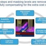
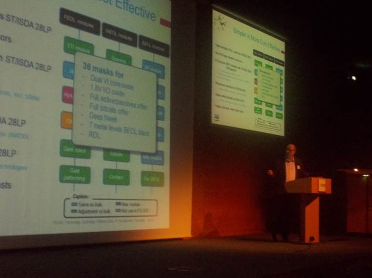
Finally, I will talk about the presentation made by Giorgio Cesana, Technical Marketing Dr with STM, about FDSOI, that we can summarize by these words: FDSOI is Simpler, Cooler and Faster. When we think about SOI, we remind the technology used by AMD ten years ago or the exotic ASIC products developed for military application. According with ST, FDSOI is, in 2013, completely different, as it’s now Simpler (planar devices to be compared with 3D FinFET), with an immediate impact in term of mask count, generating itself a direct impact on technology cost. The SOI wafers are more expensive? True! But you need less process steps and less masks (even when comparing with Bulk 28nm), so the cost evaluation per wafer is within 1% between 28FDSOI and Bulk28LP… When comparing 14FinFET and 14FDSOI wafer cost, FDSOI appears to be 35% cheaper!
If you remember this blog, you already know why FDSOI is “Cooler”, or “Faster”, thanks to Silicon On Insulator technology, the power consumption is minimized compared with Bulk. Because you can run a microprocessor faster by 20% or more, using the same power budget: FDSOI is Faster. In fact, this is just the first slides summary, so I will have to come back to FDSOI in one next blog. I had the opportunity to discuss with Giorgio, so I will have the possibility of writing well documented blog about FDSOI, stay tuned!
From Eric Esteve from IPNEST
More Articles by Eric Esteve …..