eSilicon Corporation was founded in 2000 with Jack Harding as the founding CEO and Seth Neiman of Crosspoint Venture Partners as the first venture investor and outside Board member. They both remain involved in the company today, with Jack continuing as CEO and Seth now serving as Chairman of the Board.
Both Harding and Neiman brought important and complementary skills to eSilicon that helped the company maneuver through some very challenging times. Prior to eSilicon, Jack was President and CEO of Cadence Design Systems, at the time the largest EDA supplier in the industry. He assumed the leadership role at Cadence after its acquisition of Cooper and Chyan Technology (CCT), where Jack was CEO. Prior to CCT, Jack served as Executive Vice President of Zycad Corporation, a specialty EDA hardware supplier. He began his career at IBM.
Seth Neiman is Co-Managing Partner at Crosspoint Venture Partners, where he has been an active investor since 1994. Seth’s investments include Brocade, Foundry, Juniper and Avanex among many others. Prior to joining Crosspoint, Seth was an engineering and strategic product executive at a number of successful startups including Dahlgren Control Systems, Coactive Computing, and the TOPS division of Sun Microsystems. Seth was the lead investor in eSilicon, and incubated the company with Jack at the dawn of the Pleistocene epoch.
THEEARLYYEARS
eSilicon’s original vision was to develop an online environment where members of the globally disaggregated fabless semiconductor supply chain could collaborate with end customers looking to re-aggregate their services. The idea was straight-forward – bring semiconductor suppliers and consumers together and use the global reach of the Internet to facilitate a marketplace where consumers could configure a supply chain online. The resultant offering would simplify access to complex technology and reduce the risk associated with complex design decisions.
Many fabless enterprises had struggled with these issues, taking weeks to months to develop a complete plan for the implementation of a new custom chip. Chip die size and cost estimates were difficult to develop, technology choices were varied and somewhat confusing, and contractual commitments from supply chain members took many iterations and often required a team of lawyers to complete.
The original vision was simple, elegant and sorely needed. However, it proved to be anything but simple to implement. In the very early days of the company’s existence, two things happened that caused a shift in strategy. First, a close look at the technical solutions required to create a truly automated marketplace yielded significant challenges. Soon after formation of the company, eSilicon hired a group of very talented individuals who did their original research and development work at Bell Labs. This team had broad knowledge of all aspects of semiconductor design. It was this team’s detailed analysis that lead to a better understanding of the challenges that were ahead.
Second, a worldwide collapse of the Internet economy occurred soon after the company was founded. The “bursting” of the Internet bubble created substantial chaos for many companies. For eSilicon, it meant that a reliable way to monetize its vision would be challenging, even if the company could solve the substantial technical issues it faced. As a result, most of the original vision was put on the shelf. The complete realization of the “e” in eSilicon would have to wait for another day. All was not lost in the transition, however. Business process automation and worldwide supply chain relationships did foster the development of a unique information backbone that the company leverages even today. More on that later.
THEFABLESSASIC MODEL
Mounting technical challenges and an economic collapse of the target market have killed many companies. Things didn’t turn out that way at eSilicon. Thanks to a very strong early team, visionary leadership and a little luck, the company was able to redirect its efforts into a new, mainstream business model. It was clear from the beginning that re-aggregating the worldwide semiconductor supply chain was going to require a broad range of skills. Certainly design skills would be needed. But back-end manufacturing knowledge was also going to be critical. Everything from package design, test program development, early prototype validation, volume manufacturing ramp, yield optimization, life testing and failure analysis would be needed to deliver a complete solution. Relationships with all the supply chain members would be required and that took a special kind of person with a special kind of network.
eSilicon assembled all these skill sets. That deep domain expertise and broad supply chain network allowed the company to pioneer the fabless ASIC model. The concept was simple – provide the complete, design-to-manufacturing services provided by the current conventional ASIC suppliers, such as LSI Logic, but do it by leveraging a global and outsourced supply chain. Customers would no longer be limited to the fab that their ASIC supplier owned, or their cell libraries and design methodology.
Instead, a supply chain could be configured that optimally served the customer’s needs. And eSilicon’s design and manufacturing skills and supply chain network would deliver the final chip. The volume purchasing leverage that eSilicon would build, coupled with the significant learning eSilicon would achieve by addressing advanced design and manufacturing problems on a daily basis would create a best-in-class experience for eSilicon’s customers.
As the company launched in the fall of 2000, the fabless ASIC segment of the semiconductor market was born. Gartner/Dataquest began coverage of this new and growing business segment. Many new fabless ASIC companies followed. Antara.net was eSilicon’s first customer. The company produced a custom chip that would generate real-world network traffic to allow stress-testing of ebusiness sites before they went live. Technology nodes were in the 180nm to 130nm range and between eSilicon’s launch in 2000 and 2004, 37 designs were taped out and over 14 million chips were shipped.
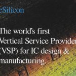
Fabless ASIC was an adequate description for the business model as everyone knew what an ASIC was, but the description fell short. A managed outsourced model could be applied to many chip projects, both standard and custom. As a result, eSilicon coined the term Vertical Service Provider (VSP), and that term was used during the company’s initial public exposure at the Design Automation Conference (DAC) in 2000.
eSilicon’s positioning, DAC 2000
The model worked. eSilicon achieved a fair amount of notoriety in the early days as the supplier of the system chip that powered the original iPod for Apple Computer. The company also provided silicon for 2Wire, a company that delivered residential Internet gateways and associated services for providers such as AT&T. But it wasn’t only the delivery of “rock star” silicon that set the company apart. Some of the original ebusiness vision of eSilicon did survive.
eSilicon’s first logo. The squares symbolize the end product – the chip
The company launched a work-in-process (WIP) management and logistics tracking system dubbed eSilicon Access[SUP]®[/SUP] during its first few years. The company received a total of four patents for this technology between 2004 and 2010. eSilicon Access, for the first time, put the worldwide supply chain on the desktop of all eSilicon’s customers. Using this system, any customer could determine the status of its orders in the manufacturing process and receive alerts when the status changed. eSilicon uses this same technology to automate its internal business operations today.
GROWINGTHEBUSINESS
During the next phase of growth for the company, from 2005 to 2009, an additional 135 designs were taped out and an additional 30 million chips were shipped. Technology nodes now ranged mainly from 90nm down to 40nm. It was during this time that the company began expanding beyond US operations. Through the acquisition of Sycon Design, Inc., the company established a design center in Bucharest, Romania. A production operations center was also opened shortly thereafter in Shanghai, China.
Recognizing the growing popularity of outsourcing, eSilicon expanded the VSP model to include semiconductor manufacturing services (SMS). SMS allowed fabless chip and OEM companies to transition the management of existing chip production or the ramp-up and management of new chip production to eSilicon. The traditional design handoff of the ASIC model was now expanded to support manufacturing handoff. The benefits of SMS included a reduction in overhead for the customer as well as the ability to focus more resources on advanced product development.
Extensions such as SMS caused the Vertical Service Provider model to expand, creating the Value Chain Producer (VCP) model. The Global Semiconductor Alliance (GSA) recognized the significance of this new model and elected Jack Harding to their Board to represent the VCP segment of the fabless industry.
In the years that followed, up to the present day, eSilicon has grown substantially. The number of tape-outs the company has achieved is now approaching 300 and the number of chips shipped is on its way to 200 million. The company has also expanded into the semiconductor IP space. While its worldwide relationships for third-party semiconductor IP are critical to eSilicon’s success, the company recognized that the ability to deliver specific, targeted forms of differentiating IP could significantly improve the customer experience.
Since so many of today’s advanced chip designs contain substantial amounts of on-board memory, this is the area that was chosen for eSilicon’s initial IP focus. The company acquired Silicon Design Solutions, a custom memory IP provider with operations in Ho Chi Minh City and Da Nang, Vietnam. This acquisition added 150 engineers to focus on custom memory solutions for eSilicon’s customers.
As of June 30, 2013, eSilicon employs over 420 full-time people worldwide, of which over 350 are dedicated to engineering. Headquartered in San Jose, California, the company maintains operations in New Providence, New Jersey and Allentown, Pennsylvania; Shanghai, China; Seoul, South Korea; Bucharest, Romania; Singapore and Ho Chi Minh City and Da Nang, Vietnam. The company’s diverse global customer base consists of fabless semiconductor companies, integrated device manufacturers, original equipment manufacturers and wafer foundries. eSilicon sells through both an internal sales force and a network of representatives.
THEEVOLVINGMODEL
The eSilicon business model has evolved further. VSP and VCP are now SDMS (semiconductor design and manufacturing services). Arguably the longest, but perhaps the most intuitive name. Through the years, eSilicon has allowed a broad range of companies to reap the benefits of the fabless semiconductor model, many of which couldn’t have done it on their own.
This ability to bring a worldwide supply chain within reach to smaller companies gave eSilicon its start, but the model has worked well for eSilicon beyond these boundaries. Today, eSilicon serves customers that are much larger than eSilicon itself; customers that could “do what eSilicon does.” In the early days, the company discounted its chances of winning business at an enterprise big enough to maintain an “eSilicon inside.”
Time has proven this early thinking to be too limiting. Many of eSilicon’s customers today can clearly maintain an “eSilicon inside,” but they still rely on eSilicon to deliver their chips. Why? In two words, opportunity cost. It has been proven over time that for any enterprise the winning strategy is to focus on the organization’s core competence and invest in that. All other functions should be outsourced in the most reliable and cost-effective manner possible. Simply put, eSilicon’s core competency fits in the outsourcing sweet spot for many, many organizations. This trend has created new value in the fabless semiconductor sector and facilitated many new design starts.
WHAT’SNEXT
As the fabless model grows, there are new horizons emerging. During its early days, the vision of using the Internet to facilitate fabless technology access and reduce risk was largely put on the shelf. The reasons included the challenges of solving complex design and manufacturing problems and the lack of a clear delivery mechanism over the Web.
Today, these parameters are changing. The Internet is now an accepted delivery vehicle for a wide array of complex business-to-business solutions. eSilicon’s talented engineering team has also developed a substantial cloud-enabled environment that is used to automate its internal design and manufacturing operations every day. This team consists of many of the same people who highlighted the challenges of addressing these issues in the company’s early years. What a difference a decade can make.
What if that automated environment could be made available to end users in a simple, intuitive way? New work at eSilicon is taking the company in this direction. The recent announcement of an easy-to-use multi-project wafer quote system is an example. What once could take two weeks or more, consisting of many inquiries and legal agreement reviews, is now done in as little as five minutes with an extension to eSilicon Access. With availability on both the customer’s desktop and smartphone, this is clearly the beginning of a new path. eSilicon changed the landscape of fabless semiconductor in 2000 with the introduction of the fabless ASIC model. It’s time to do it again and bring back the “e” in eSilicon.