RVN! 26 Banner revised (800 x 100 px) (600 x 100 px)

Macro Placement Challenges

Macro Placement Challenges
by Paul McLellan on 12-27-2013 at 7:28 pm

One of the challenges of physical design of a modern SoC is that of macro placement. Back when a design just had a few macros then the flooplanning could be handled largely manually. But modern SoCs suffer from a number of problems. A new white paper from Mentor covers Olympus-SOCs features to address these issues:

  • As we move to smaller technology nodes we can put a lot more functionality on the same die. Not perhaps quite as much as you want since metal fabric is not scaling as fast as historically. The varying aspect ratios of the macros make it difficult to pack them tightly without wasting silicon area. Designers are left with the challenge of running multiple iterations to identify a reasonable configuration to take through full place and route.
  • Poor seed placement. Floorplan designers typically run multiple trials using various seed placement configurations with the hope of finding the ideal solution. Since the quality of the initial placement is rarely optimal, you see an increase in both the number of trials with various seed placements and also the number iterations with the pre-CTS runs.
  • Design space exploration. Conventional tools lack the ability to perform early design space exploration that considers various design metrics such as timing, area, leakage power, and congestion. This leads to inferior seed placement and also to performance and area being left on the table. There is typically no automated method to collate and present the results of all the trial macro placements done, so there is no way to make an informed decision on the full-blown implementation.
  • Missing macro analysis functionality. Traditional tools provide very primitive macro analysis capabilities for determining whether a certain placement configuration is best suited for implementation. The analysis engines typically do not have the intelligence to analyze the connectivity through multiple sequential stages. Another drawback is that if a macro placement already exists for a block based on legacy design experience, the analysis functionality is either not supported or is very minimal. In order to determine the best placement, it is critical to have very powerful analysis and incremental what-if analysis capabilities.
  • Pre clock-tree synhesis (CTS) optimization After getting the initial seed placement, there are typically many cycles iterating through the full blown pre-CTS flow to analyze timing, area, congestion and other design metrics before choosing a configuration for implementation. Because the seed placement QoR is often sub-par, the design needs to be analyzed to determine the feasibility of closing the design or block, which involves launching multiple trials in parallel. The pre-CTS runs are costly both in terms of resources and time, but can be eliminated with a good quality seed placement.
  • The result of these problems causes more iterations and as a result the time to accomplish timing closure increases.


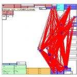
Olympus-SoC offers a completely automated macro placement (AMP) technology for both block level and hierarchical designs that delivers the best QoR in the shortest time. It offers tools for design space exploration to make the right trade-offs to meet various design metrics like timing, area, and congestion. AMP includes powerful what-if macro analysis capabilities for fine tuning macro placement results. The AMP flow significantly reduces the design time and eliminates weeks of manual iterations.

Olympus-SoC’s AMP technology offers the following features:

  • Data flow graph driven macro placement and legalization
  • Design space exploration with customizable recipes for parallel exploration
  • Powerful macro analysis and refinement
  • Completely automated flow with minimal manual intervention

The white paper covers the flow through the graph driven macro placement engine, how to assess quality of macro placement, refining the placement. There is a small case study.

The white paper is here.


More articles by Paul McLellan…


Get into a Xilinx FPGA for Under $90

Get into a Xilinx FPGA for Under $90
by Luke Miller on 12-27-2013 at 6:30 pm

Jump into Xilinx Programmable Logic today! I wanted to encourage my dear readers if you have not tried using an Xilinx FPGA (Field Programmable Gate Array) or even CPLD (Complex Programmable Logic Device) then it is worth your time to begin your evaluation. Maybe you got one for Christmas? If not, it is easier than you think to start exploring the wonderful world of Xilinx!

For many, even the non-nerdy folk, know what a CPU, GPU are etc… But the FPGA remains in the shadows at times, but I would like to highlight some suggestions that will allow you to, without much money and effort to enter into the World of Xilinx programmable Logic Devices. While Xilinx is certainly the world’s FPGA leader, with the Virtex-7, 28 nm a huge success, coupled with Zynq (Dual ARM devices and even a leg) and the 20nm UltraScale family, boasting 5500+ DSPs and 64 GT’s, things are looking wonderful for Xilinx. But maybe you don’t need all that horsepower and are just curious and want to learn more without a heavy investment of time and money.

So how do you try Xilinx Programmable Logic? To the outsider, things can feel scary, hearing things like VHDL, Verilog, Synthesis, Place and Route, Constraints, Timing Closure. In fact it can feel overwhelming. Well the good news is it is not as hard as one may think. Most of us in our FORTRAN, BASIC (or Abacus for some of you ;)) days had to write the ‘Hello World’ Program. The equivalent of the ‘Hello World’ for the Xilinx Programmable Logic in my humble opinion is the ‘blinking LED’. For the Blinking LED to occur, many successful steps were taught and caught and the LED winking at you will just propel you to want to learn more and more of the multidimensional world of Xilinx FPGAs.

Like anything new there is a learning curve but I am convinced that once you start playing with the Xilinx FPGAs you will have more ideas of designs that you would like to implement. The possibilities are endless as Xilinx FPGAs do not tie you down to any particular standard. You program or design the interface, you design the algorithms. It could be SPI, RS-232, PCIe, Fiber, 10,100 GbE feeding a video tracking algorithm for, well whatever tickles you’re fancy. The point is you can control more than just some functions, you own the space, the IO, the RAM, the DSP.

Today, you can get into a Xilinx board from $89 from Diligent, Avnet has the MicroZed for $199, and Adapteva has the Zynq based Parallella Board for $99. They come with the necessary software license to begin playing with your Xilinx FPGA board. What you’ll find is that you have a blank piece of canvas in the form of Silicon. What do you want it do? Once you are comfortable with the Xilinx FPGA board and the tool flow you’ll really be wondering why you did not do this sooner. There are literally unlimited resources, forums, groups that are creating a growing Xilinx FPGA community. So what will you create? Check outXilinx.com for more details on all there Programmable Logic Solutions and some of the aforementioned boards above to see what you may have been missing.

More articles by Luke Miller…

lang: en_US


Patterns looking inside, not just between, logic cells

Patterns looking inside, not just between, logic cells
by Don Dingee on 12-27-2013 at 5:00 pm

Traditional logic testing relies on blasting pattern after pattern at the inputs, trying to exercise combinations to shake faults out of logic and hopefully have them manifested at an observable pin, be it a test point or a final output stage. It’s a remarkably inefficient process with a lot of randomness and luck involved.

Getting beyond naïve (typified by the “walking 0 or 1” or transition sequences such as hex FF-00-AA-55 applied across a set of inputs) and random patterns hoping to bump into stuck-at defects, computational strategies for automated test pattern generation (ATPG) began modeling logic looking for more subtle faults such as transition, bridging, open, and small-delay. However, as designs have gotten larger, the gate-exhaustive strategy – hitting every input with every possible combination in a two-cycle sequence designed to shake both static and dynamic faults – quickly generates a lot of patterns but still fails to find many cell-internal defects.

A new white paper from Steve Pateras at Mentor Graphics explores a relatively new idea in ATPG that challenges many existing assumptions about finding and shaking faults from a design.

Cell-Aware Test

A cell-aware testapproach goes much deeper, seeking to target specific defects with a smaller set of stimuli. Rather than analyzing the logic of the design first, cell-aware test goes after the technology library of the process node. It begins with an extraction of the physical library, sifting through the GDSII representation looking at transistor-level effects with parasitic resistances and capacitances. These values then go into an analog simulation, looking for a spanning set of cell voltage inputs (still in analog domain) that can expose the possible faults.

After extending the simulation into a two-cycle version looking for the small-delay defects, the analog simulation is ready to move into the digital domain. The list of input combinations is converted into necessary digital input values to expose each fault within each cell. With this cell-aware fault model, now ATPG can go after the gate-level netlist using the input combinations, creating a much more efficient set of patterns to expose the faults.

A big advantage of the cell-aware test approach is its fidelity to a process node. Once the analog analysis is applied to all cells in a technology library for a node, it becomes golden – designs using that node use the same cells, so the fault models are reusable.

But how good are the patterns? Pateras offers a couple pieces of analysis addressing the question. The first is a bit trivial: cell-aware patterns cover defects better in every cell, by definition from the targeted analysis. The second observation is a bit more surprising: for a given cell, cell-aware analysis actually produces more patterns in many cases compared to stuck-at or transition strategies, but detects more defects per cell.

Play that back again: the cell-aware test approach is not about reducing pattern count, but rather about finding more defects. Pateras presents data for cell-aware test showing on average, the same number of patterns shakes out 2.5% more defects, and a 70% increase in patterns gets 5% more defects. Those gains are significant considering those defects are either all blithely passing through device level test, or requiring more expensive screening steps such as performance margining or system-level testing to be exposed.

The last section of the paper looks at the new frontier of FinFETs, with a whole new set of defect mechanisms. Cell-aware test applies directly, able to model the physical properties of a process node and its defects. A short discussion of leakage and drive-strength defects explains how the analog simulation can handle these and any other defects that are uncovered as processes continue to evolve.

For finding more defects, cell-aware test shows significant promise.

More articles by Don Dingee…


Smart Watch, Phone, Phablet, Tablet, Thin Notebook…?

Smart Watch, Phone, Phablet, Tablet, Thin Notebook…?
by Pawan Fangaria on 12-26-2013 at 12:30 pm

There are more, but wait a while, from this set which ones do you need? Or let me ask the question differently (I know you may like something impulsively and have money to buy), which ones do you want to buy and own? Still confused? I guess what you need, you already have, but you want to change it for something new and different. While I talk about some more, functionally different, fancy wearable things later, let me analyse these ones to help making a rational decision.

When I first saw an SmartWatch advertisement, all these devices flashed through my mind and I had been thinking to write an article on this topic from user’s point. After reading Beth Martin’s article, “The hottest real estate? Your wrist!”, I couldn’t wait anymore.

So, what’s there in a SmartWatch? It has most of what you have in your SmartPhone or less than that. But because it’s wearable, you don’t have to carry it in your pocket. Carrying something is a problem! Yes, that’s the problem with laptop too; one has to carry it in a separate case. And so, most of the laptop functionality started getting into SmartPhone (so that you don’t have to carry a separate case) and it became smaller and smaller to fit into your pocket, until it was realized that we need a bigger screen for applications like reading or compiling a document. So, we now see a trend of having larger screen on SmartPhone!!


Where do we go from here, a Phablet, Tablet or Notebook again? Well, a Phablet is a negotiation between a phone and a tablet, although not easily pocket-able, but manageable. Talking about impulse buying, Tablets came in as a huge success with fantastic customer demand as that was easy to handle with touch keyboard. It was a fancy among school going kids, I guess it still is. But that market for Tablets is vanishing, taken away by Phablets and now thin sleek Notebooks.

With larger screen of a Notebook, one has great convenience of working, like in an office, and that cannot be ruled out. The negatives are being mostly eliminated by the emergence of thinner and lighter Notebooks with better screens, hybrid form factors, ergonomics and longer battery life. That eliminates another inconvenience of carrying a Bluetooth keyboard along with a Tablet.

Coming back to the question, which all devices can be laden on our body, pocket or bag? My opinion – the new ultra-thin Notebooks (like MacBook Air and Lenovo Yoga) will make a comeback in our bags and SmartPhones will remain evergreen in our pockets. SmartWatch and other wearable devices will not be mainstream products, they need a careful approach to target the appropriate segment and position the smart product smartly for that segment. It’s okay to be as geek devices for that matter.

For a SmartWatch to position itself well, it must have important features meaningful to the user, such as health monitoring, fitness tracking, built-in GPS, a battery life of about a month, wireless charging, better with a self-charging solar cell and other nifty features. Emulating a SmartPhone on that small screen may be a mistake. In age-old wrist watch positioning, niche segment of Rolex and Rado is still ruling and there are many in mainstream segment. And we have seen the death of digital watches which had arrived with a big bang in the past.

FuelBand, Nike’ssporty brand, can be a strong contender for that real estate of your wrist, specifically for athletes and sports enthusiasts. Then there are other uncommon wearable devices such as SmartBra (by Microsoft), clearly targeted towards women; Sproutling Fitness Tracker for babies, clearly useful for mothers of small babies; and there are others like SmartWig (by SONY), Google Glassetc. Imagine a SmartWig that sits on your head containing various sensors to track your brain activities, blood pressure, temperature, vibrator to signal a phone call etc. and then camera, speakers, GPS and so on. Are you ready to wear it whole day long and expose your brain to all that radiation?

Time to think what you want to wear, what you want to keep in your pocket and what you want to carry in your bag!! Eliminate one over the other if its functionality (as needed by you) is completely overlapped by the other and that makes you easy to go!! Happy investing in your personal technology 🙂

More Articles by Pawan Fangaria…..

lang: en_US


Highest Test Quality in Shortest Time – It’s Possible!

Highest Test Quality in Shortest Time – It’s Possible!
by Pawan Fangaria on 12-26-2013 at 10:30 am

Traditionally ATPG (Automatic Test Pattern Generation) and BIST (Built-In-Self-Test) are the two approaches for testing the whole semiconductor design squeezed on an IC; ATPG requires external test equipment and test vectors to test targeted faults, BIST circuit is implemented on chip along with the functional logic of IC. As is evident from the ‘external and internal to an IC’ approaches, both have unique advantages and limitations.

By using ATPG any digital design chip can be tested with high quality covering wide variety of defect detection and fault models such as stuck-at, transition, bridge, path-delay, small-delay etc. However, it requires large number of test patterns to get high fault coverage. And 99% and more fault coverage is a norm in today’s complex chip design to sustain required quality. Therefore, compressed test data is stored in the tester and is applied to the chip scan chains put between a de-compressor and a compactor, thus speeding up the test and requiring lesser tester memory.

On the other hand logic BIST can be used in any environment (without the need of any tester) for designs that need re-test on system. This proves to be very important for system self-test in critical applications such as satellite, automobile or flight control systems. It’s a very practical approach for plug-and-play design support with short test time, provided the design is not pseudo-random resistant. In an internal arrangement, a pseudo-random pattern generator (PRPG) generates test patterns which pass through the scan chains and the responses are collected in a multiple input signature register (MISR) that determines the pass or fail by comparing to the expected signature. This approach has less coverage on faults that need special targeting unlike ATPG.

Again, in ATPG, a FF capturing a wrong value (due to design issue) can be masked at a mild loss of fault coverage. But in logic BIST, entire chain between the PRPG and MISR will need masking for such cases. Logic BIST cannot tolerate any unknown value (due to any non-scan instance) whereas ATPG can ignore any unknown value at the tester. That means a higher design impact in case of BIST insertion than in ATPG compression.


So what should be the best strategy to attain maximum coverage in shortest possible test time? As we can see, ATPG and BIST can be used to complement each other, and both offering more common features these days, Mentorhas exploited these into a hybrid approach by combining the logic from embedded compression ATPG and logic BIST (LBIST).


[Hybrid shared test logic with top-level LBIST controller to manage clocking and sequencing of LBIST tests]

Most common logic of the two test methodology is merged, thus saving in area. Compression ATPG and LBIST are shared within each design block and there is an additional LBIST controller at the top level. In this approach, ATPG needs to target only those faults that are not already detected by LBIST, thus saving test time significantly.

This hybrid approach which can be used in top-down as well as bottom-up design flow, saves hardware cost as well as test time and provides highest fault coverage. Also, in case of bottom-up flow Mentor’s Tessent TestKompress can re-use the patterns previously generated at the core level, thus saving in test pattern generation time.

EDA vendors such as Mentor provide tools to re-use logic between embedded compression ATPG and LBIST. A whitepaperat Mentor’s website provides a great level of detail about ATPG, LBIST and the hybrid approach of test strategies. Interesting read!!

More Articles by Pawan Fangaria…..

lang: en_US


A little FPGA-based prototyping takes the eXpress

A little FPGA-based prototyping takes the eXpress
by Don Dingee on 12-26-2013 at 9:00 am

Ever sat around waiting for a time slot on the one piece of big, powerful, expensive engineering equipment everyone in the building wants to use? It’s frustrating for engineers, and a project manager’s nightmare: a tool that can deliver big results, and a lot of schedule juggling.

Continue reading “A little FPGA-based prototyping takes the eXpress”


SLEC is Not LEC

SLEC is Not LEC
by Paul McLellan on 12-20-2013 at 3:00 pm

One of the questions that Calypto is asked all the time is what is the difference between sequential logical equivalence checking (SLEC) and logical equivalence checking (LEC).

LEC is the type of equivalence checking that has been around for 20 years, although like all EDA technologies gradually getting more powerful. LEC is typically used to verify that a netlist implementation of a design corresponds to the RTL implementation (although more rarely it can be used for RTL to RTL, and netlist to netlist verification). However, LEC suffers from a major restriction: the sequential behavior of the design must remain unchanged. Every register and every flop in one of the designs must correspond exactly to an equivalent one in the other. Tools vary as to how restrictive they are about whether the registers need to be named the same. And this is not quite true, there are a few simple transformation that RTL synthesis does that a typical LEC tool can handle, such as register retiming (whereby logic is moved across registers and might invert the register contents in a very predictable way).

SLEC is used when the sequential behavior is not the same or when the high level description is completely untimed C++ or SystemC and so the sequential behavior is not fully described. The three most common cases where this can happen are:

  • a tool such as Calpyto’s PowerPro is used to do sequential power optimization. It does this by suppressing register transfers when the results are not going to be used, but this completely changes the sequential behavior at the register level, although if everything is done correctly it should not change the behavior of the block at the outputs. SLEC is used to confirm that this is indeed the case
  • a high level synthesis (HLS) tool such as Catapult is used to transform a design from a C/C++ description to RTL. SLEC can check that the HLS tool created functionally correct RTL from the high level input
  • a high level C/C++ description of the design is automatically or manually transformed into another C/C++ description (perhaps to make it synthesize better) and SLEC can be used to ensure this transformation did not introduce any errors

So stepping back to the 50,000 foot level, LEC is used to check that logic synthesis tools have done their job correctly (and these days logic synthesis is buried inside place and route so it is not just the pure front end tools that are involved). It can also be used to check that manual changes made at that level (such as hand optimizing some gates) is done correctly.

SLEC is used to check that high level synthesis tools have done their job correctly or that other tools such as PowerPro that make sequential changes have done their job correctly.

By combining both technologies gives you complete end to end verification from high level description through the various tools that change the design, all the way down to netlist.


More articles by Paul McLellan…


Semicon Technology Advancement – A View From IEDM

Semicon Technology Advancement – A View From IEDM
by Pawan Fangaria on 12-20-2013 at 10:00 am

As I see the semiconductor industry going through significant changes and advances, yet ironically plagued by a growing perception that the pace of scaling is slowing, I was inclined to take a peek into what the industry experts say about the state of the industry and the future of Moore’s Law. Fortunately, at last week’s International Electron Devices Meeting (IEDM 2013), a panel discussion among an impressive lineup of experts from industry leading organizations was set up. Dr. David M. Fried, CTO-Semiconductor at Coventor, the host organization, moderated the session.

[Panel – In the Trenches: Insights from Experts on Advanced Technology Development. From left, facing the audience – Dr. David M. Fried (addressing the audience), Dr. Laith Altimime, Dr. Sean Lian, Dr. Brian Greene, Dr. Andy Wei, Dr. Herve Jaouen]

The discussion was structured around defining the greatest technical challenge, and looked further into where to find answers. Generally speaking, the greatest challenge was identified as keeping development of increasingly complex integration schemes on schedule and within budget and how the industry can align to address it. Several panellists added personal details to exemplify the challenge. Dr. Brian Greene, 14nm FEOL architect at IBM, highlighted adoption of new device architectures and materials and increasing process-module interdependencies as challenges. Dr. Sean Lian, Director and Technology Lead at Samsung, is assessing all the schemes to scale down to the 7 nm technology node. Dr. Herve Jaouen, Director of Modelling & Simulation at ST, sees challenges in Middle-of-Line optimization and complex design rules. Dr. Andy Wei, Process Architecture PMTS at GLOBALFOUNDRIES, added that managing patterning costs is a major part of the challenge.

Where to find answers to this challenge? It was a unanimous opinion to find it through closer ties between design and process technology development, industry collaboration, university research and process simulation. There are many variables that must be optimized to keep development on schedule, such as test mask design and optimally allocating resources for fundamental research of advanced technology nodes (e.g. 7nm). Dr. Andy Wei looked up to the EDA tools industry to help meet some of these challenges and accelerate the pace of development.


[Collaboration through semiconductor ecosystem, Government and Universities]

How can the industry help? An obvious answer is collaboration within the semiconductor industry ecosystem and with government and research institutions (universities). Dr. Laith Altimime, Director of CMOS Technology & Design at IMEC, stressed that maximizing leverage of the full ecosystem is essential. He referred to this as “The Sum of Minds”. Dr. Brian Greene observed that physical process modelling and advanced inline metrology and defect detection can also help. Also, Dr. Herve Jaouen anticipated that process trials will always help.

I would consider process modelling as crucial help from within the industry ecosystem. And that reminds me about the SEMulator 3D Virtual Fabrication Platform; an innovative solution from Coventor that can address many of these challenges — such as reducing long process-design cycles, long build-and-test learning cycles, vetting process integration ideas, quantifying allowable process module variation and so on. Although it’s off the panel (I wasn’t present in IEDM), it prompts me to ask Dr. David M. Fried certain questions in the context of this discussion –

Q: I think your SEMulator3D tool can help keep the schedule of semiconductor design development, to a large extent. What do you think has to be done more?

A typical silicon learning cycle costs $50M and lasts three months. The industry needs to explore new ways to do things instead of doing the same thing harder and faster. For example, there are an increasing number of big branch decisions during pre-silicon exploration that cannot tolerate this cost or time. Virtual fabrication is a way to take a massive step forward in the rate and pace of silicon development. In early development, virtual fabrication can be used to explore new process ideas in a matter of days instead of months. As the technology approaches manufacturing, virtual fabrication can be used to optimize process control and ramp yield. In both cases, computational time is the only cost.

Q: I see collaborative research either within the industry or with universities can definitely help with advancing the technology and meeting the existing and upcoming challenges. Are you doing some collaboration in that direction to enrich your existing offerings or introduce new offering?

We have numerous on-going university and industry collaborations. We have found that our deepest collaborations benefit both sides most. At the most basic level, getting more minds together is essential to solving the complicated integration issues the industry is faced with today. The deep collaborations lead to understanding technical challenges and delivering solutions faster. Seeing how the industry uses our virtual fabrication platform allows us to continually improve the usability and predictivity of our product.

Q: I know from our earlier discussion that you are working on 3D design rules. To what extent can these rules ease technical challenges for MOL, BEOL or FEOL processes?

We recently released a new functionality called “Structure Search” which evaluates the entire 3D model for structural failure mechanisms. This is an enormous leap forward from the industry’s prevailing method of creating design rules in spreadsheets with limited capability to account for process variation or interactions. The ability to use 3D models that predict exact process variation increases confidence in the design rules and reduces the time required to validate them. Structure Search also enables verification of the special constructs required for designs to leverage the advanced technology nodes we are working on today.

Q: One last question, you say parallel technology tracks such as FinFETs versus FD-SOI makes collaboration difficult. How do you see this in the light that one is simpler and cost effective and the other is complex to process, but may prove to provide better results? Isn’t it worth to validate the results before coming onto a single track?

I don’t think the comparison between those technologies is that cut-and-dry. Both come with their own set of challenges. The division of resources and focus to examine the two technology tracks is another example of how the industry needs to focus on performing development differently. FinFET versus FD-SOI is a big branch decision at the technology level and virtual fabrication should be leveraged here for exploration and comparison. There is still a lot of work ahead to evaluate the two tracks. If there is going to be a clear winner, virtual fabrication is one tool that can decrease the time to make this decision.

It was my great pleasure interacting with Dr. David M. Fried after getting the view from IEDM. This gives a true picture of the way semiconductor technology is going to advance in near future and new ways and tools to help that process. Happy reading!!

More Articles by Pawan Fangaria…..

lang: en_US


EDA and Semi IP Stocks in 2013: MENT, ARMH, CDN, SNPS, ANSS, CEVA, IMG.L

EDA and Semi IP Stocks in 2013: MENT, ARMH, CDN, SNPS, ANSS, CEVA, IMG.L
by Daniel Payne on 12-20-2013 at 12:39 am

2013 was an up year for the stock markets as both the DJIA and the tech-heavy NASDAQ showed significant growth, so how did EDA and Semi IP companies do in the past 12 months? A quick stock plot from Yahoo Finance shows us that only two of the seven companies beat the NASDAQ: ARMH, MENT.


Continue reading “EDA and Semi IP Stocks in 2013: MENT, ARMH, CDN, SNPS, ANSS, CEVA, IMG.L”