RVN! 26 Banner revised (800 x 100 px) (600 x 100 px)

Semiconductor IP and Correct-by-construction Workspaces

Semiconductor IP and Correct-by-construction Workspaces
by Daniel Payne on 01-21-2014 at 8:00 pm

SoC hardware designers could learn a thing or two from the world of software development, especially when it comes to the topic of managing complexity. Does that mean that hardware designers should literally use a software development environment, and force fit hardware design into file and class-based software methodologies? I don’t really think so, but it would make sense for hardware designers to use some best practices from software development that have been adapted to the unique IP-centric world of SoC design where it’s becoming more common to use hundreds of IP blocks.

A workspace is the name give to environment where SoC design including IP content and the metadata used to describe it are managed, and changes to IP are tracked. You could manually create workspaces and then manually track IP changes with a general purpose tool like Excel, however it would likely consume weeks of valuable engineering effort and the results would be error prone because you would have to manually alert other designers on your team every time a change to IP was made.

Manually managed workspaces introduce more issues like: the security of certain IP and who should have access, selecting the correct IP versions to avoid errors, and keeping network traffic and disk usage at a minimum.

Correct-by-construction Workspaces

Now that we know the risks of using a manual process, let’s define what a correct-by-construction workspace methodology should do for us:

  • Centralized Management of all IP, where any change is automatically propagated to anyone of the design team.
  • Centralized security by assigning the proper access to each IP block by each team member.
  • Minimized disk usage by using a common, read-only version of IP blocks.
  • View management where a designer can see all data views required.
  • Multi-site support so that teams spread around the globe can see and use the IP to get their projects completed with a minimum latency, low network traffic and low disk storage.

Hardware design is not Software design

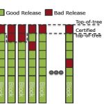
Chip designers run regressions, simulations and physical verifications that can take from minutes to days, and can consume large amounts of RAM and disk space, so it’s not practical to treat this like an Agile software development process that relies upon a “top-of-tree” approach. For SoC design a feasible approach is to to track which blocks have been fully verified in the context of the whole design, then add that to a certified top-of-tree:

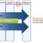
ProjectIC from Methodics

Engineers at Methodicshave created ProjectIC as a platform to manage the IP lifecycle for both chip and IP designs that does create and track correct-by-construction workspaces.

One commonality between software and hardware development is that ultimately they are just collections of files. Popular data management tools like Perforce can be used for both hardware and software disciplines, however additions must be made to support an IP-centric design methodology. Hardware designs need to track IP metadata and have an IP abstraction layer enabled by IP metadata to be effective:

Features on top of data management for ProjectIC that enable correct-by-construction workspaces are:

  • An IP catalog to list which IP release can be used.
  • Central definitions so that you can control IP configurations for your design.
  • Security through permissions control.
  • Task specific workspaces for an IP block being designed.
  • View management so that an RTL designer doesn’t need to check out the physical layout view.
  • Automatic notifications of any new IP block release to anyone that is using that block.
  • Minimized disk space usage by having remote or local data available to a workspace.

Further Reading

There’s a four page white paper from Methodics that goes into more detail and it can be downloaded here. There you’ll read about:

  • Workspace management in practice
  • Creating a workspace
  • Editing Local IP data
  • Releasing an IP
  • Managing defects
  • Improved collaboration

Another related white paper is called Data Management Best Practices, which covers how to effectively use DM for hardware design. There’s a brief registration process before you can download either white paper.

Conclusion

A correct-by-construction workspace approach will save you time, effort and provide peace of mind over a manually managed workspace methodology.


DSPs converging on software defined everything

DSPs converging on software defined everything
by Don Dingee on 01-21-2014 at 5:00 pm

In our fascination where architecture meets the ideas of Fourier, Nyquist, Reed, Shannon, and others, we almost missed the shift – most digital signal processing isn’t happening on a big piece of silicon called a DSP anymore.

It didn’t start out that way. General purpose CPUs, which can do almost anything given enough code, time, power, and space, were exposed as less than optimal for DSP tasks with real-world embedded constraints. In order for algorithms to thrive in real-time applications, some kind of hardware acceleration was needed.

The DSP-as-a-chip emerged, with tailored pipelining and addressing modes wrapped around multiply-accumulate stages, and in more modern implementations larger word widths and parallelism. Popular general purpose DSP families from Analog Devices, Freescale, TI, and others still exist today, making up about 8% of market revenue according to Will Strauss.

What happened? As DSP became part of more systems, technology diverged targeting specific portions of a system with its capability, in the mix with other more general purpose resources. Four other methods enabling signal and image processing algorithms appeared:
[LIST=1]

  • Programmable logic and IP, in FPGAs from Altera and Xilinx et al,
  • In-line vector instructions, such as ARM NEON or Freescale AltiVec or Intel AVX,
  • Vector execution units, typical of modern GPUs from AMD and NVIDIA,
  • IP cores for SoCs, including those from CEVA, Coresonic, or Cadence Tensilica.

    For every divergence, there is a convergence. Today, flexibility for more than one application is the name of the game, and that is breaking the boundaries between device types. GPUs are morphing into more than just graphics engines, CPUs want to do some DSP algorithms, and DSPs and FPGAs both crave partner cores for more general purpose work.

    This is giving rise to new combinations of general purpose cores and DSP capability for acceleration of key functions. Looking at recent multicore developments – TI KeyStone, Xilinx Zynq, NVIDIA Tegra K1 to name a few – the trend is becoming obvious. By no means does this imply these parts are exactly interchangeable, just that the trend is headed away from the traditional DSP-as-a-chip toward a multicore blend of functions.

    So, it shouldn’t be a surprise these influences are also changing how DSP IP cores are evolving, getting beyond specialized point functions such as audio and baseband interface. By definition, a DSP IP core sits astride an ARM or other processor core, fitting into the trend we’ve identified. This brings opportunities in interconnect and cache coherency, along with new possibilities.
    In a marked departure from the traditional DSP architecture, CEVA has uncorked the XC4500, with features borrowed from almost all the approaches we’ve talked about converging in a single part. Paul McLellan introduced us to the XC4500 last fall, but I’ll mention two items briefly. First is a vector processing element, able to rip through over 400 16-bit operations in a single cycle. Second is the interface between the vector engine and several CEVA-defined plus open to user-defined co-processors, which CEVA terms “tightly coupled extensions”.

    It’s a huge jump from DSP point functions in mobile handsets into a crowded field of wireless infrastructure solutions. Will CEVA succeed here? We should keep in mind the Internet of Things is driving us into new territory: software defined everything. Just as the DSP-on-a-chip is no longer the entire processor, the radio is now no longer the entire product. Efficient operation in the space between subscribers and the cloud is going to require a lot more than just protocol engines and baseband processing, and the workload-tuned CEVA XC4500 is another good example of processor evolution.

    My guess is what we will see from CEVA and others is a learning cycle or two, where these new DSP architectures continue to evolve, and new application ideas emerge as the right combinations of features and ways for partner cores to use them are discovered. Designers will have to get used to multiple, formerly separate disciplines of thinking – DSP plus vector engine plus ARM core, all tied together via software, being a good example – and how to best partition and coordinate software to achieve system goals.

    At the spot software defines everything, the new DSP convergence will probably be found.

    More Articles by Don Dingee…..

    lang: en_US


  • Happy Birthday GSA

    Happy Birthday GSA
    by Paul McLellan on 01-21-2014 at 2:57 pm

    This year marks the 20th anniversary of GSA and collaboration around the foundry and fabless ecosystem. Originally GSA was FSA, the fabless semiconductor association. There was a semiconductor associations 20 years ago, the SIA, but that was still the “real men have fabs” era and fabless semiconductor companies were not considered “real” semiconductor companies and so were excluded. Now, of course, nobody would claim companies like Qualcomm, Broadcom, Xilinx are not real semiconductor companies. Going forward, only Intel and Samsung have their own fabs to build their own chips. And both of them also have at least some foundry business and so participate in the fabless ecosystem too.

    During the year each month there GSA will be producing video interviews with industry leaders discussing GSA. The first one is features Steve Mollenkopf of Qualcomm, Scott McGregor of Broadcom, Mark Edelstone from Morgan Stanley and more.

    GSA also has 2 technical working group meetings this week that are open for registration.
    What: 3DIC Packaging Working Group Meeting
    When: Wed, JAN 22, 2014 | 2:00 PM – 5:00 PM
    Where: Altera, 101 Innovation Drive, San Jose, CA 95134
    Why: The industry is developing 3D-IC related standards to help ensure interoperability and minimize development time. The Q1 3DIC Working Group meeting will focus on:

    • Altera’s 3D-IC Strategy with Arif Rahman, Architect
    • Standards update from Si2, SEMI, and IPC

    Register here

    What: IP Working Group Meeting
    When: Thurs, JAN 23, 2014 | 9:00 AM – 12:00 PM
    Where: Synopsys, 700 E. Middlefield Road, Bldg 8, Mountain View, CA, 94043
    Why: Widely used interfaces help drive IP development, and MIPI technology, used in mobile applications, is such an interface. The Q1 IP Working Group meeting will cover:

    • MIPI organization will discuss how their standards efforts help drive IP development.
    • IEEE-ISTO Nexus 5001™ will discuss on-chip instrumentation and the impact on IP development.

    Register here


    More articles by Paul McLellan…


    Smart Clock Gating for Meaningful Power Saving

    Smart Clock Gating for Meaningful Power Saving
    by Pawan Fangaria on 01-21-2014 at 5:30 am

    Since power has acquired a prime spot in SoCs catering to smart electronics performing multiple jobs at highest speed; the semiconductor design community is hard pressed to find various avenues to reduce power consumption without affecting functionality and performance. And most of the chips are driven by multiple clocks that consume about 2/3[SUP]rd[/SUP] of total chip power. So what? In a simplistic manner, it’s very easy to visualize the solution as, “gate the clock on registers to be active only when they are needed to drive any activity”. However, there are different tricky scenarios which need to be looked at in order to do it correctly. Also, imagine you discovered the clocks to be gated at the layout stage in a multi-million gate design, how difficult and expensive it would be modify the design?

    What if we have a tool that can automatically identify the clocks to be gated at right places in right manner and at the earliest stage, i.e. RTL? SpyGlass Power is such a versatile tool that can find gating opportunities, estimate effectiveness in saving power, fix problems at RTL, and check the design for correctness and testability while providing other important features such as reporting various statistics (e.g. no. of enabled registers Vs. time graph, power enable score card, power saving report etc.) which can be utilized by the designers to make informed decisions.

    Above is an example where upstream registers are gated while downstream registers are driven by free clock. Enable at the upstream registers can be delayed and used to gate the downstream registers as well without affecting the functionality.

    Another example shows how a recursive approach is needed to find all clock gating opportunities in the design. By tracing forward from register ‘A”, gating opportunities at register “B” can be found, but not at “C” simultaneously. The gating opportunity at “C” can be found only after the opportunity at “B” has been found.

    How to determine whether a clock gating will really be effective in saving power? Considering this example, in order to save large power consumption in operators such as multipliers and comparators, one could think of adding clock gating at the upstream register, but that would mean duplicating the downstream enable logic at upstream enable also. This defeats the purpose of power saving. SpyGlass Power computes power consumed before and after gating and allows designers to implement only those gating scenarios that save power significantly, because gating has costs in terms of additional delay and more work for clock tree synthesis.

    Another important, rather critical aspect to look at is that the clock gating must not introduce any meta-stability issues on Clock Domain Crossing (CDC) for asynchronous clocks. SpyGlass Power is intelligent enough to infer meta-stability issues and avoid them in order to implement only CDC-safe clock gating.

    SpyGlass Power also helps synthesis tools (which use register width as a factor to implement clock gating) to avoid bad clock gating. It computes actual power saving due to enables and generates a “don’t touch” script for negative power opportunities which can be used by the designers to guide their synthesis tool appropriately.

    A power enable scorecard report, like the one above, provides unique opportunity for a designer to look at the areas where there is more room for clock gating and also inefficient clock gating which does not save much power. “mc_cont” has ~98% of clock activity saving (with ~40% of registers gated), but still has 96 more new gating opportunities. An opposite scenario in “mc_rf” shows ~90% of registers gated, yet only ~1% of clock activity saving.

    After finding the right opportunities to add clock gating, SpyGlass Power can fix them automatically in most commonly used RTL descriptions such as Verilog, SystemVerilog or VHDL. By looking at the detailed reports and highlighted schematics, a designer can also find more gating opportunities and fix them manually.

    After fixing the code for gating all possible clocks, it becomes obligatory to re-verify the new power optimized RTL. It’s not wise to do a full blown simulation at this moment, nor a standard Logic Equivalence Checking (LEC) because it does not understand sequential changes. SpyGlass Power provides Sequential Equivalence Checking (SEC) that can verify the equivalence between original and new RTL much faster.

    Above is a complete flow of power estimation, reduction, fix, and re-verification of RTL description in SpyGlass Power. Also, there is SpyGlass DFT DSM to further verify the clock gated design for correct propagation of test clocks through various modes such as scan shift, capture, and at-speed capture. SpyGlass CDC is another tool to verify a complete design to make sure there are no functional issues across asynchronous clock domains.

    Guillaume Boillet and Kiran Vittal have described the overall scheme of operation in more detail with specific examples in their whitepaperposted at Atrenta website. I loved studying it and would recommend designers and semiconductor professionals to read it through and know more.

    More Articles by Pawan Fangaria…..

    lang: en_US


    Digital @ Nano-Scale while Analog Hovers @ 65nm and Above

    Digital @ Nano-Scale while Analog Hovers @ 65nm and Above
    by Daniel Nenni on 01-20-2014 at 9:00 pm

    Who’s going to DesignCon next week? I am, absolutely. Dr. Hermann Eul, Vice President & General Manager, Mobile & Communications Group, Intel Corporation will be keynoting on Tuesday. This one I want to hear! Intel missed mobile at 32nm, 22nm, and 14nm. Lets see what they have planned for 10nm. Something good I hope!

    Want to meet me? I will be on a panel in the Overcome Analog and Mixed-Signal Design and Verification Challengessession. Here is the abstract:

    There’s a growing schism in the world of mixed-signal IC design. This stems from the increasing rate and pace of digital designs being created at deeper nano-scale process nodes while analog designs continue to hover at process nodes of 65, 90 and larger. Requirements both technological and business/market have a large influence on this division. Digital designers are under intense pressure to increase functionality and reduce cost , which drives higher chip density and reduced chip footprint. In contrast, analog requirements may call for high voltages or advanced RF capabilities that necessitate the larger process nodes. This all converges at the foundry where designs are transposed to silicon. How are foundries and EDA vendors addressing and/or overcoming this challenge? What design types and application areas are most likely to have to navigate this divide? How are design kits (PDKs) and other design enablers helping to mitigate the issue?

    The Great Divide: Digital @ Nano-Scale while Analog Hovers @ 65nm and Above

    Zhimin Ding | Anitoa Systems
    Jeff Miller | Product Manager, Tanner EDA
    Dan Nenni | Founder, SemiWiki.com
    Mahesh Tirupattur | Executive Vice President, Analog Bits, Inc
    John Zuk | VP Marketing & Business Strategy, Tanner EDA

    Session Code: 2-WE7
    Location: Ballroom E
    Date: Wednesday, January 29
    Time: 3:45pm-5:00pm

    Session attendees will engage with experts from A/MS foundries & EDA tool vendors to discuss the growing divide between digital and analog design. Digital designs are racing down the process node path with current tape-outs at 20nm and roadmaps to 14 and 10nm. Mainstream analog and mixed-signal designs continue to tape out at 90, 180nm and above. Here, the long-term implications of this schism will be discussed.

    Created by engineers for engineers, DesignConis the largest gathering of chip, board and systems designers in the world and is focused on the pervasive nature of signal integrity at all levels of electronic design – chip, package, board and system. Combining technical paper sessions, tutorials, industry panels, product demos and exhibits, DesignCon brings engineers the latest theories, methodologies, techniques, applications and demonstrations on PCB design tools, power and signal integrity, jitter and crosstalk, high-speed serial design, test & measurement tools, parallel & memory interface design, ICs, semiconductor components and more.

    DesignCon enables chip, board and systems designers, software developers and silicon manufacturers to grow their design expertise, learn about and see the latest advanced design technologies & tools from top vendors in the industry, and network with fellow engineers and design engineering experts.

    More Articles by Daniel Nenni…..

    lang: en_US


    The Semiconductor Landscape – III

    The Semiconductor Landscape – III
    by Pawan Fangaria on 01-20-2014 at 12:30 pm

    In continuation to my earlier observations and anticipations (landscape1, landscape2) which came up to my expectations, I was further inspired to ponder over the macros of our ever growing semiconductor industry. We may argue the business is stagnating, we may argue that the pace of scaling is slowing, but when I look back at the year bygone, I can clearly see a thoughtful trend of consolidation in the semiconductor arena, and that is extended to even the semiconductor manufacturing equipment business. At the same time there is expansion in areas which are poised to drive the semiconductor industry going forward. Smart move!

    Looking at 2013, it appears that semiconductor industry is turning around, as we see growth numbers trending towards positive ~5.2% (as per Gartner’s estimate based on world’s top10 semiconductor vendors revenue – 2012 rev $299,912M; 2013 rev $315,390M) from decline in earlier years. According to SIA (Semiconductor Industry Association) report the latest Nov 2013 rev has increased to $27.24B from $25.51B in Nov 2012, a healthy ~6.8% increase. This shows a healthy trend in store for future. Revenues from home appliances and its adjacent areas such as sensors, touch controls, smart meters etc. (not to forget smart phones :)) particularly in emerging un-saturated markets has been on the rise. Then there’s a tremendously large market of internet-of-things beaconing at us in the near future.

    Having talked about a little bit on macroeconomics of semiconductors let me delve into the next level of strategic affairs in the industry. I will use my pet lenses of Business leadership, Technology leadership and IP leadership.

    So, from business leadership angle, I can see consolidations among semiconductor businesses (EDA, IP, design and foundry) along with some of the adjacent areas like semiconductor equipment companies (AMAT acquiring TEL), Microsoft acquiring Nokia and Google about to buy Nest Labs which makes thermostats and smoke detectors. Without going into details with several examples, I would like to point out one distinct pattern of strengthening IP portfolio by large organizations. We know ARM is the leader in IP business. Now we see EDA veterans, Synopsys and Cadence strengthening significantly in this area through several acquisitions over last two years. It’s obvious, that’s an area to fuel growth in semiconductor industry, through internet-of-things in future.

    As I had talked about IP leadership in my last article, IP is the brain child of semiconductor industry, it has its own will on whether to join with large magnets or flourish independently. While some of the niche IP organizations have joined hands with large organizations, there are others are doing well and many new IP vendors mushrooming steadily. So, this area will always be ripe, although ridden by heavy competition going forward. What will boost IP business further is internet-of-things market with very aggressive time-to-market schedules.

    Coming to technology leadership – this is an interesting area, it leads business. Whenever, there is concentration in a particular business, technology takes a look from a distance and re-organizes itself to move forward from there. While we see foundries looking at 7nm node, FinFET or FD-SOI, there are other avenues growing to take More’s law further through 3D-IC. Newer tools are coming up to handle manufacturing complexities through newer, faster and cost effective methods such as Virtual Fabrication. EDA vendors are moving up the chain to handle large SoC and 3D designs through newer means such as major design decisions and sign-offs done at RTL level and maturing the tools down the line to handle everything automatically.

    Looking at economics taking a growth trajectory, we can expect semiconductor industry going through significant leap with newer technologies, newer designs, newer methods and tools and newer market collaterals in the near future. Let’s be optimistic!

    More Articles by Pawan Fangaria…..

    lang: en_US


    SilabTech Awarded 2013 Best Start-up in India

    SilabTech Awarded 2013 Best Start-up in India
    by Eric Esteve on 01-20-2014 at 8:32 am

    This is obviously great news for SilabTech, and this is the type of news which will change the perception that we (non-Indian) have of the Semiconductor industry in India. About 15-20 years ago, the India Embedded/VLSI industry was perceived as low cost design resource pool, a good place where to implement design center. The hidden insinuation was that decision power was located in western countries… This is still probably true for multinational companies, except that the cost is no more the main criteria why to rely on India based design center, as the quality of experienced designers is now the major reason to relocate design operation in India!

    If we look at the winners list of the Mentor Graphics(R) Leadership Awards for the Embedded/VLSI Industry, we see that only Qualcomm and Microchip (two out of seven) are multinational (the full list at the end of this post):

    The winners for this year, by category, are:
    — Best VLSI/ Embedded Design — Automotive:
    TVS Motors;
    — Best VLSI/ Embedded Design — Consumer Electronics:
    Ineda Systems;
    — Best VLSI/ Embedded Design — Defense/Aerospace:
    SCL, Chandigarh;
    — Best VLSI/ Embedded Design — Telecom/Networking:
    Qualcomm;
    — Best VLSI/ Embedded Design Company from the Sub-Continent:
    Millennium IT;
    — Best Electronic System Design Company — Multinational:
    Microchip;
    — Best Electronic System Design Company — Startup:
    Silab Tech;

    It’s to be noticed that the panel of judges are eminent business leaders:

    Sanjay Nayak, CEO & MD,Tejas Networks;
    Krishna Moorthy K, MD – India Design Center, Rambus Chip Technologies;
    Santhanakrishnan Raman, Managing Director, LSI India R & D;
    Guru Ganesan, President & MD, ARM-India Operations;
    Dr. S. Jabez Dhinagar, VP – Advanced Engineering Group, TVS Motors;
    and Sunil Thamaran, Managing Director-Cypress India.

    These judges are mostly coming from multinational companies like Rambus Chip Technology, LSI Logic, ARM or Cypress: their decision to select a majority of India based design companies (and not multinational R&D subsidiaries) is a clear sign that times are changing. Indian semiconductor ecosystem is moving from low cost design service area it was in the 1990’s to a country of entrepreneur, starting Design IP or Electronic System companies, as it appears to be today. Who say this? Walden C. Rhines, CEO and chairman, Mentor Graphics: “These award-winners showcase India’s rich resource of electronic design talent,” “This talent, combined with a spirit of innovation and a strong entrepreneurial drive, is what makes India an exciting place for the electronic information future,” said Walden C. Rhines, CEO and Chairman, Mentor Graphics.

    If we come back to SilabTech example, the company has been built around a team of very experienced analog designers, involved in PLL and High Speed SerDes IP. SilabTech is still in start-up mode, although not involved into a start-up “gambling model” where you create a company and staff it as fast as possible as the goal is a fast exit through acquisition. SilabTech is targeting the long term development, investing wisely when needed: the first Interface IP (USB 3.0, PCIe gen-3, MIPI M-PHY to name a few) have been developed in 28nm technology. Because Silicon proven IP is a must have for such advanced nodes supporting expensive chip development, SilabTech has implemented these IP in a Test Chip (first and third above pictures), so they can claim having Silicon Proven IP. This is everything but a low cost strategy! SilabTech is currently developing a 12,5 Gbps SerDes to be released to Silicon soon…

    Times are changing and India based design companies (not only design services companies) are emerging, like SilabTech, following a start-up model closer to US than to China, using VC money rather than money coming from government. The next step will be the emergence of India based Fabless semiconductor, no doubt that we will see fabless coming soon to join this dynamic ecosystem.

    To read the full PR on the Wall Street Journal, go here

    Semiwiki readers already know about SilabTech… remember this article

    By Eric Esteve from IPnest

    lang: en_US


    More Articles by Eric Esteve …..


    Intel is NOT Transparent Again!

    Intel is NOT Transparent Again!
    by Daniel Nenni on 01-19-2014 at 9:00 am

    Recent headlines suggest that Intel was not transparent about some of the products they showed at the CES keynote. Intel confirmed on Friday that they used ARM-based chips for some of the products but would not say which ones. When your company’s tag line is “Intel Inside” and you hold up a product during your keynote wouldn’t one assume that Intel was actually inside?

    Today saying someone is not transparent really means they are being deceptive and when that someone is the CEO of a publicly traded semiconductor company it is serious business, my opinion. Even more glaring is the Intel claim of a 35% density advantage over TSMC at 14nm. This was presented during the November 21[SUP]st[/SUP] 2013 Intel analyst meeting. There is a barely noticeable disclaimer in the bottom right corner that says:

    Sources: TSMC keynote, ARM Tech Con 2012, Oct. 30, 2012. Intel data alignment based on internal assessment.

    This goes to my argument that Intel is NOT serious about the foundry business. They used a trade show marketing presentation from 2012 for this technical analysis? Is that the best the mighty Intel can do for competitive information?

    Based on a thorough investigation by myself and just about every other company in the fabless semiconductor ecosystem this claim has proven to be absolutely FALSE. I write this now so when silicon is out and scrutinized we can go back and see who was telling the truth. Spoiler alert: It is not Intel!

    The other interesting Intel news is that their big 14nm fab in Arizona will not be in production anytime soon. The delay was called a “minor correction”. The real reason for the delay, in my opinion, is so that Intel can continue to claim 80% capacity utilization so Wall Street does not downgrade INTC stock. If Intel counted idle fabs, their capacity numbers would be closer to 50% than 80%.

    The other big news is that TSMC 20nm is in full production. We already knew this but it is nice to see TSMC talking about it:

    “We have two fabs, fab 12 and fab 14 that complete the core of the 20nm-SoC. As a matter of fact, we have started production. We are in the [high]-volume [20nm] production as we speak right now,” said C. C. Wei, co-chief executive officer and co-president of TSMC, during a conference call with investors and financial analysts.

    Do you remember last year TSMC said on a conference call that 20nm would be in volume production Q2 2014? And I said they were being cautious, that it would happen in Q1 2014? I know things, believe it. TSMC also said 20nm will account for 10% of wafer revenues in 2014 which would be more than $2B worth of 20nm wafers.

    TSMC also did a FinFET update:

    Talking at the company’s latest financial meeting, Mark Liu, TSMC co CEO, claimed its 16nm FinFET process is now ready for tape out and could be in volume production this year. “Our 16FinFET yield improvement has been ahead of our plan. This is because we have been leveraging the yield, learning from 20SoC. Currently, the 16FinFET SRAM yield is already close to that of the 20SoC process.”

    Let’s not forget what Mark Bohr of Intel said about TSMC last year:

    “Bohr claims in TSMC’s recent announcement it will serve just one flavor of 20nm process technology is an admission of failure. The Taiwan fab giant apparently cannot make at its next major node the kind of 3-D transistors needed to mitigate leakage current, Bohr said.”

    TSMC 16nm is a FinFET version of 20nm, right? Maybe Mark saw that in a marketing presentation years ago? Intel, you really are better than this. If you don’t have something transparent to say maybe you should say nothing at all.

    More Articles by Daniel Nenni…..

    lang: en_US


    Managing Heat for System Reliability

    Managing Heat for System Reliability
    by Pawan Fangaria on 01-17-2014 at 8:30 am

    In most of the electronic equipments, semiconductor chips are a major source of heat generation. And in semiconductor designs several hardware and software techniques are being used to contain power dissipation; a major cause for heat. However due to multiple functionality being squeezed into small form factors, we continue to experience our electronic devices such as smartphone, notebook and other networking and telecom devices that operate continuously, getting heated up after prolonged use. It’s essential to manage that heat to disperse through appropriate enclosure design, cooling, heat sink and other techniques; otherwise even a single chip failure can render the whole system at risk. How to model those designs for cooling of electronic devices which pose several complexities such as sheer number of solid-fluid and solid-solid surfaces, material property, highly cluttered for air circulation etc.?

    It was a positive surprise for me coming across this state-of-the-art tool, FloTHERM XT from Mentor. I really admire the versatility of offerings from Mentor across all spheres of semiconductor design from chip and package to complete system, applicable to diverse set of applications including automotive, aerospace and defense.

    FloTHERM XT takes EDA and MDA (Mechanical Design Automation) design flows together from concept to product validation, thus minimizing the risks associated with thermal aspects of the design as early as possible. It uses a solid modelling engine that can create a 3D model of the product with the desired level of details to keep the electronic and mechanical design in sync. This unique tool is easily used by design as well as thermal experts who can analyse the system through plenty of what-if scenarios.

    FloTHERM XT provides an easy-to-use GUI to build models, automatic meshing, and efficient simulation of complex systems and convergence that significantly reduces overall time spent on thermal simulation compared to any CFD (Computational Fluid Dynamics) based solution.

    The whole process is best described through a case study in a whitepaper at Mentor’s website.


    [FloTHERM XT – Thermal design flow – Concept to prototype for electronic products]

    The design starts with a simple representation of a PCB and components. An initial assessment of temperatures of critical components and cooling strategy is made. And then a complete model of the system is developed in stages with required enclosure and heat sinks designed through MCAD. Interface resistances are added and the full board layout is imported from EDA via FloEDA bridge. After merging enclosure from MDA system and PCB from EDA system, a thorough thermal simulation is performed. The component modelling also evolves through the flow; thermal models can change in complexity as required. FloTHERM XT has advanced library swapping and filtering support to choose appropriate models. The detailed modelling of IC packages is also done to determine if critical junction temperatures are exceeded.

    Since power dissipation has increased and products are more compact than ever, thermal designs have become critical bringing EDA and MDA design flows closer together. FloTHERM XT provides a rapid design environment to create model geometry do simulation and develop the best optimized prototype to be manufactured. It has semi-automatic, object based algorithms, with options to adjust the mesh manually where required.

    A detailed study of the thermal design issues, complexities involved in CFD based systems and how FloTHERM XT solves those issues in simplistic terms for the user is described in the whitepaper. It’s a good read for thermal, electronic, automotive, aerospace, and defense design engineers.

    More Articles by Pawan Fangaria…..

    lang: en_US


    JasperGold COV App, the Swiss Army Knife for Verification

    JasperGold COV App, the Swiss Army Knife for Verification
    by Paul McLellan on 01-16-2014 at 12:55 am

    At the Jasper Users Group meeting in October Rajeev Ranjan presented on the JasperGold COV App which he described as the Swiss army knife for verification. It comes in many sizes and contains many useful tools.

    The primary goal of COV is to provide coverage metrics:

    • stimuli coverage: how restrictive is the design behavior under the formal set up?
    • property completeness coverage: how complete is the property set?
    • proof coverage: what coverage is achieved by the proven properties?
    • bounded proof coverage: what is the coverage and is it enough?


    That last item, bounded proof, is used when only a subset of the state-space can be traversed and no violation is encountered. But it is not a full proof. A bounded proof of K cycles implies that all states reachable within K cycles of the reset state have been analyzed and all possible events with K cycles have been triggered.


    It is also integrated in with the simulation database since formal doesn’t live in a verification world of its own and assertions that are covered by simulation do not need to be covered by formal and vice-versa. There is a special flow that can be used to improve simulation coverage with the unreachable coverage target detection flow, whereby JG coers items that are not hit in simulation and also confirms items that are unreachable and thus cannot be covered by simulation.

    Different companies use the tool in different ways. Customers include Broadcom, ST, ARM, Applied Micro, Juniper, Nvida and others. Different usage models include:
    [LIST=1]

  • Verification coverage for bounded result (property checking, sequential equivalence checking)
  • Completeness of property set
  • Protecting against over-constraint, dead-code analysis
  • Verification coverage from full-proof analysis
  • Post-silicon debugging
  • Detect and eliminate unreachable cover targets for simulation
  • Assist simulation in reaching a hard to reach target

    Another facet is protection from over-constraints. Assumptions (constraints) limit the set of legal stimuli but assumptions can interact in complex ways resulting in conflict (not easily identifiable by eyeballing). This leads to the danger of false confidence for proven properties and so should always be used as a sanity check for all the proven properties. A special case is identifying dead code that cannot be reached, which can often lead to very fast identification of RTL bugs early in the design cycle.

    There is more in the presentation. If you are a Jasper user (not necessarily one who attended JUG) then you can download the presentations, including this one, here.


    More articles by Paul McLellan…