Synopsys IP Designs Edge AI 800x100

Robust Design <- Robust Flow <- Robust Tools

Robust Design <- Robust Flow <- Robust Tools
by Pawan Fangaria on 08-10-2013 at 6:00 pm

I could have written the sequence of the title in reverse order, but no, design is the one which initiates the need of a particular flow and the flow needs support of EDA tools to satisfy that need. It’s okay if the design is small; some manual procedures and workarounds/scripts may be able to perform certain jobs. However, as the design becomes complex and its size increases, it needs systematic, established, fast, accurate and automated set of steps which can complete the chip in a reasonable time and provide high yield.

This week, it was another interesting opportunity for me, listening to a DAC 2013 presentation (in the form of a webinar) of GLOBALFOUNDRIES in association with ANSYS-Apache. It’s a typical collaboration in semiconductor industry where a chip designer as a customer and an EDA tool provider as a supplier work closely as a team throughout the design cycle to produce something whose end consumer is several chains down the line.

[Simplification of blocks by abstraction – schematic diagram]

Dr. Hendrik Mau of GLOBALFOUNDRIES explained in very simplistic terms about the complexity of their power-gated, multi-domain design at 20nm node and how they have been able to abstract it into simpler blocks to determine the overall IR drop within acceptable limits of accuracy and reasonable time. It’s a 64Mbit SRAM with 128 blocks, 6528 power domains and more than 2.3M pratio entries per block. Now determining 6528 internal power nets and analyzing IR drop at transistor level for VMIN (the minimum voltage at which an array of bits can successfully be written and read at a specified yield target) characterization of the design is a huge task. Even a tool, if run on flat design will consume more than 512GByte of main memory and several days to complete. So, there come the techniques to simplify blocks by abstraction and use hierarchical approach with the assistance of automated tools to do the jobs at each step. As we see in the picture above, a block can be simplified into a coarse block that reduces the number of power domains and restricts analysis up to a higher level of metal.

[Flow established at GLOBALFOUNDRIES]

In the above flow, Calibre from Mentor has been used for extraction of hierarchical netlist, which specifies actual locations and orientations of the cells. Apache tools have been used in the successive steps. APLMMX finds out all internal power nets connected to transistors, reads extracted netlist and generates GDSII files. APLSW does switch cell characterization and generates model for the switch depicting actual resistance. Then Totem reads in GDSII file and generates LEF/DEF for the blocks and the top level. Now Totem reads the LEF/DEF and the switch cell model to generate the IR drop.

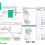
[Hybrid Approach – GDSII view and view in Totem; IR drop results of 64Mbit SRAM]

GLOBALFOUNDRIES used a hybrid approach having 4 fine blocks in the middle surrounded by 124 coarse blocks. IR drop in metal M6 with all blocks consuming same power and whole design connected through wire bond is elliptical, where as it is increased in M1 and M2 in the fine blocks at the center.

[Comparison of run time and memory requirements in flat and hybrid approach]

The hierarchical hybrid analysis of a smaller design of size 8Mbit (which could be run in flat mode) with 4 fine blocks and 12 coarse blocks shows that compared to flat run it consumes lesser than 7.5x peak memory and takes lesser than 4x run time, while maximum IR drop remains close to that of the flat run.

It’s a classic example of how automatic switch tracing can simplify handling large designs and the use of hierarchical hybrid approach can reduce memory requirements and execution time for IR drop analysis. GLOBALFOUNDRIES has been able to successfully use this flow in 28nm and 20nm designs and is now using it in 14nm designs. Details about the design, flow, and tools can be found in the presentation titled “Hierarchical Voltage Drop Analysis Techniques for Complex Power-Gated Multi-Domain 20nm Designshere.


Intel Is Continuing to Scale While Others Pause

Intel Is Continuing to Scale While Others Pause
by Paul McLellan on 08-09-2013 at 11:52 am

Back in May, William Holt, EVP of technology and manufacturing at Intel gave a presentation to analysts entitled Advancing Moore’s Law, Imperatives and Opportunity. A pdf of the presentation is available here. I just saw it for the first time today and I’m not sure how to get my head around it. It starts off with a lot of historical stuff about how Intel has delivered process generations every couple of years (or maybe that the industry has, it’s not quite clear).

But the really interesting stuff is in the middle of the presentation. I have blogged before about how one of the challenges the semiconductor industry is facing going forward is that the cost per transistor is not coming down. Although there are more die per wafer at 20nm, 14/16nm etc, the cost of manufacturing that wafer is rising fast due to the increasing complexity of the process and, especially, due to the need for double patterning. The rule of thumb for a process generation in the past has been twice as many die per wafer (so a 50% reduction in area per transistor), but an increase of wafer cost by about 15% leaving 35% cost reduction left over.


But going forward, the public information available up to now has either shown no reduction in cost per transistor or even a small increase. For example, the above montage, from an ASML presentation at Semicon in July, shows data from GlobalFoundries, Broadcom and nVidia. And at the common platform forum earlier this year Gary Becker of IBM in the press Q&A said that costs per transistor will come down but “the reduction will be less than we have been used to.”

Both TSMC and GlobalFoundries 16/14nm processes basically have 20nm metal on top of a FinFET process, so there will be lots of speed/power improvements due to the improved transistors, but the effect on area scaling will be small.


As the above graph, from the Intel presentation shows, on the left there is a pause in area reduction (on the left) whereas Intel sees none since they have already done the heavy lifting to get FinFETs (that they call TriGate but I’m going to stick to the more generic term) into production at 22nm. But my understanding of Intel’s 22nm process was that it also was not aggressive on metal pitch to avoid double patterning, so I’m surprised they don’t show any flattening at all between 32nm and 22nm. Further, I suspect that the flatness of the competitor graph is exaggerated: even with the same metal pitch, faster transistors allow smaller standard cells to be used some of the time so I would expect to see some reduction in area.

As I said above, area reduction does not automatically result in a cost per transistor reduction since the cost per wafer may go up faster than the density comes down. This is especially true at 14/16nm when the metal does not shrink. Double patterning adds a to the cost for each layer that uses it. Twice through the stepper, and all the associated litho steps. For self-aligned double patterning, many more process steps to build the mandrel and remove it. But Intel sees none of this.


The cost per transistor is completely linear from 65nm down to 10nm despite the fact that at 65nm there is no double patterning and at 10nm there will need to be lots. And it is not an artifact of EUV, Intel have already said publicly that EUV is too late for 10nm.

I don’t understand how the above graph can be accurate. The cost per transistor is coming down completely linearly (actually, at 14nm they are predicting an even bigger reduction since the triangle is just below the line). As a presentation to financial analysts, this comes with all the caveats about forward looking statements, and clearly there may be unknown unknowns about 10nm. But no company is going to present data that is known to be false at the time it is presented, so I have to assume that this is an accurate (if simplified) view of Intel’s best estimate of their current and future costs.

I would like to know what TSMC, GF and Samsung think of these graphs. If they are true, Intel’s 14nm process has slightly better area than everyone else’s 10nm process (the top graph) and obviously hugely lower costs per transistor. I’m not sure I can believe it though.

Once again, Intel’s presentation is available here.


How To Connect Your Cell-phone Camera

How To Connect Your Cell-phone Camera
by Paul McLellan on 08-08-2013 at 5:31 pm

Your cell-phone contains a camera. In fact, it probably contains two: one forward facing for video-calls and one rear-facing for taking photographs and videos. The rear-facing one typically has much higher pixel count than the front-facing. The capabilities of cell-phone cameras are getting “good enough” that the point-and-shoot digital camera market is already in decline. In fact Nokia have recently announced a phone with a 41 megapixel camera, which is about 3 times the count on my point-and-shoot Canon. Lens size counts for something. A lot actually. My old 2001 era 2 megapixel Canon PowerShot G3 takes better pictures by far than my cell-phone despite having a lot lower pixel count, due to having a serious sized lens.


Since the companies that make the cameras and the companies that make the application processors (AP) are usually different, there is a need for standardization of the camera/AP interface. And the MIPI Alliance has been on top of this for several years. The main connection is a fast serial interface known as CSI (nothing to do with crime-scenes, this stands for camera-serial-interface). This consists of a D-PHY (well, two, one at each end) and a CSI-2 transmitter at the camera and receiver on the AP. The D-PHY provides the physical interface and the transmitter and receiver cover encoding, packing, error handling, lane distribution, assembly of image data stream and so on.

However the increasing size (pixel count) and frame-rate is driving the need for even higher bandwidth, hence CSI-3. Conceptually CSI-3 and CSI-2 are similar, both providing a high-speed link between camera and AP. But under the hood they are very different. CSI-3 has a new M-PHY (the successor to D-PHY) and there can be more than one on each side. Each M-PHY has a bandwidth of up to 6Gb/s per lane, with up to 4 lanes.

The next level up is the Unified Protocol layer (UniPro). This defines a unified protocol for connecting devices and components (not necessarily cameras). It is designed to have high speed, low power, low pin count, small silicon area, high reliability and so on.

Above that is the Camera Abstraction Layer (CAL) which does get specific to camera, images and video. In addition to defining how the images are transported, there is also a camera command set (CCS) extension which provides standardized mechanisms for controlling the camera sub-system.

Of course you can take the CSI-3 and M-PHY-standards and implement them yourself (I would link to them but you have to be a MIPI member to access them), just as with any other standard interface. However, when good IP is available it makes more sense to buy rather than make.

Arasan have a complete portfolio, including D-PHY and M-PHY, digital control IP (CSI-2, CSI-3, DSI etc)providing the smallest power and area footprints and the highest quality. These are customer-provoen and thus the low-risk path for fast time-to-market designs (which would be…well, all designs).

Arasan’s white paper on CSI-3 is here.

Andy Haines of Arasan will also be presenting at the Flash Memory Summit next week, although not on cameras, on Mobile Storage Designs for Compliance and Interoperability. FMS is at the Santa Clara Convention Center on Tuesday-Thursday 13-15th. Details here. And if you want to talk CSI-3 or anything else Arasan at the summit, they will be exhibiting at booth 610 and also be on the UFSA standards organization booth, which is 800.


SEMICON Taiwan 3D

SEMICON Taiwan 3D
by Paul McLellan on 08-08-2013 at 3:10 pm

SEMICON Taiwan is September 3rd to 6th in TWTC Nangang Exhibition Hall. Just as with Semicon West in July in San Francisco, there is lots going on. But one special focus is 3D IC. There is a 3DIC and substrate pavilion on the exhibit floor and an Advanced Packaging Symposium. Design tools, manufacturing, packaging and testing solutions for 2.5D-IC process are available this year, and the most important issue is how to improve its throughput to enable 2.5D-IC mass production in 2014.

3DIC is one of the key “More Than Moore” technologies to increase system capability in ways other than technology scaling (28nm, 20, 14/16 etc). Although in the long-term true 3D systems may be designed, with logic on all the layers, in the shorter term there are two particular areas showing promise:

  • 3D memories, stacking memory die, either to put them into a package like with Micron’s memory cube, or to stack memory on top of logic, probably using JEDEC’s wide IO standard
  • 2.5D interposer designs, where various chips, probably from different technologies, are flipped and attached to a silicon (or perhaps glass) interposer

Although there are some design issues with both of these, pipe-cleaner designs have successfully been done so the real roadblocks are economic.

The first economic problem is called the known-good-die problem. With a single die in a package, if a bad die slips through wafer test and gets packaged, then fails final test then you have wasted the cost of the package, the cost of putting one die in a package and bonding it out. You didn’t waste the die, it was bad anyway. Since wafer test costs money, there is a crossover point where doing more testing at the wafer stage outweigh the cost of discarding the occasional package. With a 2.5D interposer based design, a bad die that slips through means you waste a very expensive package, an interposer and all the other die in the package which were good, plus all the cost of putting everything together. It really is a lot more important that bad die do not survive that long and so the economics of wafer sort change completely.

The second economic problem is the cost of the assembly process. Wafers need to be thinned, glued to something strong enough that it can be handled, bumped, cut up, the backing removed, the die put in the package, the bumps bonded etc. If this is too expensive then it makes the whole idea of using a silicon interposer unattractive versus just using separate packages or doing some sort of multi-die bonded package.

Taiwan is ground zero of the packaging and assembly world. It has the world’s largest packaging and testing company, ASE, as well as SPIL, PTI, and ChipMOS reaching a global packaging and testing foundry market share of over 50 percent. Amkor (Korea) and STATS ChipPAC (Singapore) have also set up plants in Taiwan.

Design tools, manufacturing, packaging and testing solutions for 2.5D-IC process are available this year. So the technology is there. The most important issue is how to improve throughput to enable 2.5D-IC mass production in 2014.

Full details including registration here. 这里


TSMC is a more profitable semiconductor company than Intel

TSMC is a more profitable semiconductor company than Intel
by Daniel Nenni on 08-07-2013 at 9:00 pm

There is an interesting article on Seeking Alpha, “A More Profitable Semiconductor Company Than Intel”, and for a change the author does not PRETEND to know semiconductor technology. Refreshing! Personally I think the stock market is a racket where insiders profit at the expense of the masses. But if you are going to gamble you should do as much research as possible so you don’t end up on the wrong end of a pump and dump.

INTC was highly successful in capitalizing on the PC revolution showering investors with outsized returns. INTC, teamed up with Microsoft (MSFT) to form the famed Wintel combo that basically owned the PC market, much to shareholders delight. Alas, this is no longer 1998, and a new wave of competitors has emerged knocking INTC of its once mighty perch. The article below, will detail why Taiwan Semiconductor (TSM) is a far better play in the semiconductor space.

I certainly like how this article starts. Intel is in serious trouble and very few financial people seem to really understand it. Unfortunately, comparing Intel and TSMC is like comparing an apple to a grape since TSMC customers (AMD, QCOM, NVDA, etc…) compete with Intel not TSMC. I suggested the author do a similar comparison between Intel and Samsung since Samsung has made it very clear that they will be the #1 semiconductor company in the very near future. Considering what they have done to Apple in the mobile space, my bet is on Samsung.

Without a doubt, TSMC created what is today’s semiconductor foundry business model. While at Texas Instruments, Morris Chang pioneered the then controversial idea of pricing semiconductors ahead on the cost curve, sacrificing early profits to gain market share to achieve manufacturing yields that would result in greater long-term profits. This pricing model is still the foundation of the fabless semiconductor business model and nobody does this better than TSMC.

Today the fabless semiconductor ecosystem is a force of nature. According to IC Insights’ August Update to the 2013 McClean Report, the top 20 is now dominated by foundries, fabless, and fab-lite companies. Intel is down 4% while Qualcomm, MediaTek, and TSMC each scored more than a 20% year-over-year growth. It’s all about mobile devices. The writing is on the wall yet the Intel fan club is still calling for $30 per share. My bet would be that INTC and TSM will both be $20 stocks after FY2013 numbers are announced. But then again, I think the stock market is a racket.

lang: en_US


When Is a Good Time to Start Using High-Level Synthesis?

When Is a Good Time to Start Using High-Level Synthesis?
by Paul McLellan on 08-07-2013 at 12:42 pm

Of course if you are in the business of selling high-level synthesis (HLS) tools then the obvious answer is immediately. Start at 9am tomorrow morning. But a more realistic answer is when you are having to do something completely new. If you are working on a legacy design, perhaps with pre-existing IP, then moving the design up to a higher-level might make sense in the long-term but in the short-term it certainly comes with some costs compared to re-using what you already have in hand. But when a brand new standard comes along, there is no legacy RTL, no existing IP, and it is the perfect moment to start with a blank slate and move the level of design up another level to C++.


What is more, the standards bodies distribute their specifications as C++ reference models. OK, those reference models are not necessarily written with an efficient hardware implementation in mind, but they do introduce complex new functionality, which is something HLS is designed to make manageable. Since everything is brand new, any design team has to start from scratch and there is no downside to moving up since there is no pre-existing work being discarded.

For example, high-efficiency video coding (HEVC) also known as H.265 (pronounced aitch-dot-two-six-five) is the latest generation of mobile video compression formats. There is a lot of activity going on around HEVC and most is being done with HLS. Prior to the arrival of H.265 there was H.264 (MPEG-4, Blu-ray) which also created a surge in the adoption of HLS since it was almost impossibly complicated to implement directly in RTL. In the wireless space there has been a similar phenomenon with the introduction of 3G, LTE and WiMAX standards.

When a new standard such as H.265 is published then creating codecs is a race. HLS tools such as Calypto’s Catapult help to get that first implementation to market fast, especially compared with writing and debugging a huge amount of complex RTL from scratch.

Having got an initial implementation done using HLS, there is a subsequent benefit. Since HLS is inherently technology neutral, moving the design to a new technology node or increasing its operating frequency are straightforward. The HLS can re-synthesize the design with different libraries and constraints. It creates a new optimized RTL that matches the new process in a matter of minutes, a much simpler task than is required to move RTL to a new node with new PPA targets. Similarly, removing functionality to meet a lower price point just requires commenting out the functions that are not required.

So the answer: when starting something new, especially a new standard.

See Calypto’s blog post with more details on the topic here.


Non-volatile Memory in the Internet of Things

Non-volatile Memory in the Internet of Things
by Paul McLellan on 08-06-2013 at 9:33 pm

You have probably heard of the Internet of Things or IoT. This is the future world in which not only are our computers and smartphones connected to the internet, but all sort of other things like thermostats, medical monitors, smart car-keys and soil analyzers. What these “things” have in common is that, unlike computers and smartphones:

  • sensor-rich
  • not going to get the battery charged or changed very often, if at all
  • very low power
  • secure (encryption etc)
  • very reliable
  • many need to be very cheap


Forecasts from Cisco are that there will be 25B devices connected to the internet by 2015 and twice as many, 50B by 2020. World population today is 7B (and, amazingly, this is almost exactly the number of cell-phones in the world too).

There probably does not need to be large compute power in the device itself. Like voice-recognition in smartphones, data can be uploaded to the cloud for processing and results downloaded back again. Much lower power radios may be needed too, trading off bandwidth for power since sometimes just a few bits per day may need to be transmitted: most “things” are not going to be playing high-def youtube videos.

Think of a device that is put in place to monitor something, maybe soil moisture in the middle of a field, can run for a year without any need to change the battery, needs no maintenance, cannot be spoofed, and doesn’t cost very much since any farm might need hundreds or thousands of them. They may even be disposable, with new ones put in place for each year’s crop. That is very different from the application processor in your smartphone.

Obviously the exact details of what each device will contain will vary, but the diagram to the right is a fairly generic example. One important thing is that these devices will require some non-volatile memory for holding encryption keys, radio and sensor trim settings and, perhaps, boot code. Flash memory is too big and too power hungry. Another approach is to have an off-chip EEPROM of some sort and then upload the binary from the off-chip memory into on-chip SRAM at boot-time (and perhaps occasionally afterwards for reliability). But that requires an extra chip, maybe an extra board, more power, a bigger battery.

The best solution is one-time programmable (OTP) memory. These are very small. They can be as small as one transistor per cell. However, there may be advantages to using two transistors per cell (with one programmed to 0 and the other to 1) since then differential sensing can be used and perhaps the supply voltage lowered further. In this case, at the cost of some area, a huge power saving can result. If a memory is needed that can be programmed several times, perhaps to update encryption keys, then this can be mimicked with a larger OTP memory that is gradually filled up with the new data.

Sidense OTP technology is implemented using anti-fuses. Their memories can be manufactured in a foundry process without any changes. All the voltages required for operation of the memory are generated with on-chip charge pumps so no weird power supplies are required. The OTP technology works by causing breakdown of the gate-oxide under the fuse creating a diode. This is irreversible, whence the non-volatility. Since it doesn’t depend on storing charge the memories work over large environmental ranges and will retain their programming forever.

The Sidense white-paper on the Internet of Things is available on their website here.


What Do Brazil and Sweden Have in Common?

What Do Brazil and Sweden Have in Common?
by Paul McLellan on 08-06-2013 at 4:55 pm

Well, Sweden is not noted for its carnivals, Brazil is not noted for it’s tall blonde blue-eyed women, Sweden’s climate is not great for growing sugar cane and Brazil’s isn’t great for reindeer. Both countries speak languages with odd-sounding vowels but they are not the same language. But, ding, Jasper Design Automation has engineering organizations in both countries.


Way back in the last millennium, Tempus Fugit was founded by Vigyan Singhal and Joe Higgens. It would eventually become Jasper and Kathryn Kranen would come out of her post-Verisity semi-retirement to become CEO in 2002. The company’s headquarters is just off Castro Street in Mountain View.


In 2004, Claudionor Coelho was on the technology advisory board (TAB) of Jasper. Since he was (and is) active at the university and could direct the best students towards Jasper, they decided it would be a good idea to have and R&D office there, especially given that Brazil was very cost-effective compared with Silicon Valley. The engineering group is in Belo Horizonte (which looks like it should mean beautiful and horizontal…but this is a family blog so I’d better just move on). You probably have no idea where that is (I didn’t) but it turns out to be about a 5 hour drive north of Rio (according to Google maps, anyway).


At the end of that year, 2004, Jasper acquired a company called Safelogic in Sweden, in Gothenburg. Since I worked for a company with engineering in Sweden, meaning I had to go there regularly, I actually do know where Gothenburg is. Stockholm, where Virtutech’s engineering was (and remains, now part of Wind River which is part of Intel) is on the east coast and Gothenburg is on the west coast, about five hours driving or rather less on the train. It is the second biggest city in Sweden.


And a couple of years ago, Jasper decided to open a fourth R&D site in Israel, in Haifa. Another town I’ve actually been to, about an hour’s drive north of Tel Aviv. Before the first time I went to Israel, I thought that Jaffa and Haifa were slightly different variants on names of the same place but actually they are two completely different ports (and both seem to have some excellent restaurants).

Having engineering spread over four sites as Jasper does allows it to tap into different pools of talent. Of course Israel already has a strong technology startup culture, plus many large companies have groups there, and so good engineers are not short of options. But in Sweden and Brazil that is much less so, and exceptional engineers are keen to work at a company like Jasper.


How many consortia does POWER need to succeed?

How many consortia does POWER need to succeed?
by Don Dingee on 08-06-2013 at 1:02 pm

Sometimes press releases just make me scratch my head. Today’s example comes from IBM: after tying PowerPC and Power.org in knots for almost 20 years with rules and restrictive licensing, IBM breaks ranks and sets up ANOTHER consortium with different players.

Continue reading “How many consortia does POWER need to succeed?”


ClioSoft at GenApSys

ClioSoft at GenApSys
by Paul McLellan on 08-06-2013 at 12:51 pm

GenApSys is a biotech company developing proprietary DNA sequencing technology. As part of that they develop their own custom sequencing chips. These have an analog component and like many people they use the Cadence Virtuoso analog design environment for this.

I talked to Hamid Rategh who is GenApSys’s VP engineering. In previous companies over the last 6 years he has used ClioSoft for design data management and so with this long history it was natural that they would make that choice again at GenApSys. Not surprisingly they are very satisfied with how it works. Much of ClioSoft’s technology is tightly integrated into Virtuoso (and all the other popular layout environments if that is your thing) so that it is not necessary to spend a lot of time interfacing directly with ClioSoft explicitly. If you change a cell, it gets checked out. If you create a new version it is tracked automatically and so on.


In the old days (i think this means pre-GenApSys) there used to be some speed problems with the ClioSoft environment but that is no longer an issue. The tools is very easy to use and all the engineers are very happy with it.

Although GenApSys doesn’t do all their development at a single site, they do host all the data on a single server, so from ClioSoft’s point of view it is not a multi-site implementation. For larger companies, ClioSoft does support distribution, with a local server at each site and all of the sites kept synchronized as the design process unfurls.

ClioSoft is a small company and one of the advantages of a small company is great support. Hamid praised ClioSoft for theirs. In a tiny company, support comes directly from engineering. In a mid-sized company, support comes from application engineers. And in a large EDA company, support comes from a dedicated support organization. At each step in that ladder the support gets worse but it is more scalable. It is obvious that every engineer running into a minor issue with Design Compiler can’t call the appropriate engineer, even though he or she might provide the best response—nothing else would ever get developed.

One thing ClioSoft does that its competitors do not is to have linked workarea. This makes a big difference to the amount of disk space required. This is less of a problem than it was a disks have continued to get cheaper (even faster than Moore’s Law and due largely to completely different technology breakthroughs) although management overhead for backups etc is still an issue. And Moore’s Law is making data size explode.

So I asked Hamid to summarize their experience in a few bullets:

  • past experience was very good
  • great support
  • a tool that does exactly what is promised (DWISOTC, does what it says on the can)

Also Read

VIA Adopts Cliosoft

Agilent ADS Users, Find Out About Design Data Management

The Only DM Platform Integrated with All Major Analog and Custom IC Design Flows