llmda newsletter ad (2)

Synopsys Galaxy Platform & Lynx Design System supports FD-SOI

Synopsys Galaxy Platform & Lynx Design System supports FD-SOI
by Eric Esteve on 06-05-2014 at 11:36 am

This is a new brick that Synopsys brings to build FD-SOI credibility. We have talked at Semiwiki about FD-SOI technology developed by the LETI and STM, and recently endorsed by Samsung Foundry, offering a more than credible second source to STM. And we have said that the FD-SOI introduction will need to be supported by EDA and IP vendors to be successful. The announcement that Synopsys design flow support of 28-nm FD-SOI technology has been extended to Samsung: this simply means that SoC designers will benefit from all the design tools they need along the flow to generate a production ready IC design in GDSII format!

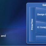
Let first take a look at the Galaxy™ Design Platform, a comprehensive solution for cell-based and custom IC implementation, Galaxy RTL and Physical implementation products concurrently balance design constraints by performing intelligent tradeoffs between speed, area, power, test and yield. Galaxy Signoff engines accurately model complex physical interactions to ensure signal and power integrity. Thus, SoC designers targeting 28nm FD-SOI can use the same design flow that they may use when targeting bulk or FinFET technologies.

Lynx Design System is built to accept various technology plug-in (left side of the picture). A technology plug-in using ST’s 28-nm FD-SOI Process Design Kit (PDK), standard cells and memories, adapts the production-proven Galaxy Design Platform-based RTL-to-GDSII flow for 28-nm FD-SOI SoC designs, accelerating project setup and execution. Lynx automation simplifies and accelerates many critical implementation and validation tasks.

A technology plug-in using ST’s 28-nm FD-SOI Process Design Kit (PDK), standard cells and memories, adapts the production-proven Galaxy Design Platform-based RTL-to-GDSII flow for 28-nm FD-SOI SoC designs, accelerating project setup and execution. Lynx automation simplifies and accelerates many critical implementation and validation tasks. “The close collaboration between ST design teams and Synopsys led to advanced silicon-proven design enablement solutions that fully leverage the performance and power promise of FD-SOI technology and provide the foundation needed to meet tight time to market windows,” said Philippe Magarshack, executive vice president, Design Enablement and Services, STMicroelectronics. “Our close collaboration with Synopsys has already enabled many successful tapeouts with mutual customers using Synopsys’ Galaxy Design Platform and Lynx Design System.”

The important word here is « foundation ». Before starting integrating CPU or DSP cores, the design team need to benefit from a complete and automated design environment, which is the case. It will be interesting to monitor the progress made by Synopsys in delivering FD-SOI proven DesignWare IP (Interfaces PHY for USB, PCIe, SATA, HDMI, the MIPI D-PHY and M-PHY, the DDR4 and LPDDR4 PHY, as well as ADC or DAC). We have highlighted in a previous post that STMicroelectronics tend to develop this type of IP, but the license agreement with Samsung does NOT includes these IP. Thus, these FD-SOI related IP represent a new segment for IP vendors like Synopsys, a TAM extension if you prefer. The right question, as of today, is whether Synopsys will port these existing above mentioned mixed-signal IP from bulk to FD-SOI straight away, or if the IP vendor will decide on a case by case basis, basing the decision on customer demand…

The comment from Dr. Shawn Han, vice president of foundry marketing, Samsung Electronics is interesting as it perfectly summarizes what was written in Semiwiki about the FD-SOI option : “28-nm FD-SOI is an ideal solution for customers looking for extra performance and power efficiency at the 28-nm node without having to migrate to 20-nm. Our close collaboration with Synopsys and ST will enable designers to reduce risk, accelerate time-to-market, minimize power and maximize performance to expand 28-nm FD-SOI adoption.”

Availability
The Synopsys Galaxy Design Platform and Lynx Design System with support for ST and Samsung 28-nm FD-SOI process technology are available now from Synopsys. The 28-nm FD-SOI-enabled PDK, standard cells and memories for early design are available now from Samsung.

From Eric Esteve from IPNEST

More Articles by Eric Esteve…..

lang: en_US


Impressions of #51DAC

Impressions of #51DAC
by Paul McLellan on 06-05-2014 at 9:56 am

So what was the overall theme of DAC this year? Usually there seems to be some trend that is hot. A few years ago it was power, then more recently all the stuff associated with 20nm and 16nm such as FinFETs and double patterning. Those things are still around, of course, and there are new generations of tools.

One theme is that more design is being done at the system level than before. The enabling technology for much of it is emulation. All three major EDA vendors have a good emulation solution. Prior to emulation the modeling problem was too big of a barrier and it was too challenging to keep the system models synchronized with the RTL. Emulation allows the RTL to be used as the model but with enough performance from the emulator to enable system level work, especially that involving software development or running software workloads.

One thing that is shaking things up a bit is Samsung’s foundry strategy. They have a clear commitment to create a foundry ecosystem that is competitive. Of course they had two big announcements in the last few weeks. Firstly was the transfer of their 14nm process to GlobalFoundries so that the identical process will be available from Samsung’s fabs in Korea and Austin and from GlobalFoundries’s fab 8 in Malta New York. Since GlobalFoundries was completely uncompetitive at 28nm it left the field open to TSMC pretty much having a monopoly for a couple of years.

Then there was the announcement that Samsung were licensing FD-SOI from STMicroelectronics. I attended a presentation by Philippe Margashack, the CTO of ST, on the Samsung booth. I already knew a fair bit about FD-SOI since I had to present on it at EDPS this year. It is available for volume production out of ST’s Crolles fab (just south of Grenoble) and will be available from Samsung early in 2015. One thing I hadn’t realized is that since FD-SOI is actually a simpler process than bulk, its cycle time is about 15% less. Another thing I learned was that the back-biasing can be used not just for power/frequency management but also to recenter the process and remove some of the variability.

TSMC were talking about their 16nm FinFET process where all the design enablement is largely complete. They are starting to talk about 10nm and are doing the preliminary work. But they also have a new process and library at 28nm. I guess one mini-theme of DAC is that 28nm is a process node that is going to stick around for a long time since it is cheap, avoids all the double patterning and variability challenges of 20nm, and has large enough capacity for many purposes. The Samsung licensing FD-SOI is another way of extending 28nm and having a better process at the same time.

Another piece of news that broke during the show was that Broadcom are getting out of mobile and selling that part of their business to Huawei. The rise of Chinese companies in mobile is somewhat underappreciated here since they mostly don’t sell in the US. But China is such a huge market on its own.

So no big overall theme for DAC this year. The march of process nodes carries on although it seems that it will be muted, with a lot of design sticking at 28nm and only the most advanced designs going to 14/16nm.

Also read: The Best and Worst of #51DAC!


Xilinx’s 16nm vs. Altera 14nm

Xilinx’s 16nm vs. Altera 14nm
by Luke Miller on 06-04-2014 at 8:00 pm

You will not believe this, but the family was picking me up Friday evening from the airport and on the way home… Get this, for real, the wife asks me to cut her hair tomorrow. Now the three of you that read my stuff, know what happened before. I resisted, and firmly said ‘No’…The wife seeing my macho stance began appealing to my engineer’s mind as she started talking economics. My dear manly readers, I stayed strong and I am out $50. Best $50 Mr. Miller spent last week…

On my travels, I learned some valuable information. One that Xilinx continues to dominate in execution, performance and design wins, and by the way, Xilinx is REALLY shipping 20nm. I must say the Xilinx competition has revealed how desperate they are, after hearing the claptrap they are pumping into the field. All I can say is “Non dolet, Paete!”

So let’s talk execution, no not the Texas kind, but did you know within hours upon receiving some wafers from TSMC that the Xilinx 20nm UltraScale Gigabit Transceivers were up and running? That is not an accident, but careful design, planning and a relationship with TSMC. The most critical choice of any FPGA company is deciding who is going to build your chips. You can have great tools, architecture and IP but that is nothing without a yielding wafer. Process, Process, process. I had the opportunity of learning ASIC design early on in life and you know what, it’s really, really hard. I would sit in meetings listening to guys with pocket protectors and crooked glasses talk about electrons and poly as if they could see them with the naked eye. Maybe they could, and that’s why the glasses were thick.

So I guess I will go here, but these are valid questions and concerns. Is Intel able to perform as a foundry? What is wrong with asking? Looking at Altera’s earning reports, the cash flowing out does not appear to be great, one could guess 50 million to Intel or even 100 million. That is not a huge amount of dough in the world of Intel, who did around 52.7 billion in sales, and let’s face it, I do not like it, as you don’t as well, but money is power and money gets things done. So, if the 4M Monolithic logic cell FPGAs start to have poor yields, who pays for that? Not just in FPGA cost and screening but how about your design schedule? How about the other Intel production runs that drive the business? Can all play nice? Can you say Errata?

Do I think Intel can pull off 14nm? No doubt, time and money fixes everything but congress. Intel’s 14nm foundry experiment need’s a guinea pig or someone to clean the foundry pipe, and frankly I would rather be the 3[SUP]rd[/SUP] customer on the Intel 14nm foundry process than the first. There is just too much that must be perfect for success to occur. While all this is going on, Xilinx is executing, Xilinx 28nm FPGAs owns more than 70% of the FPGA market, 20nm is cranking away and picking up steam, and 16nm is on deck. Do you expect there to be a hiccup on the Xilinx-TSMC well-oiled machine? Not likely, and that is why Xilinx is not only a better performing FPGA but clearly the safe choice when planning your next design, having the confidence the FPGA will be ready for action, when your design needs it, and errata free.

lang: en_US


Non-separation of power and performance

Non-separation of power and performance
by Don Dingee on 06-04-2014 at 2:00 pm

How much power does a system consume? The simplistic path to power estimation for a system used to be tossing a few metrics – standby, typical, worst case, with figures pulled from a datasheet, simulation, or physical measurement – into a spreadsheet. After filling the remaining holes with SWAG (scientific wild-ass guesses), and summing things up, there was a bottom line.

But, that bottom line on power was imprecise at best. Designers were usually after worst case, because it determined system cost. Continue reading “Non-separation of power and performance”


Ceaseless Field Test for Safety Critical Devices

Ceaseless Field Test for Safety Critical Devices
by Pawan Fangaria on 06-03-2014 at 3:00 am

While focus of the semiconductor industry has shifted to DACin this week and unfortunately I couldn’t attend due to some of my management exams, in my spare time I was browsing through some of the webpages of Cadenceto check their new offerings (although they have a great list of items to showcase at DAC) and to my pleasure I came across a really interesting, important one for this age of high-end SoCs which demand very high reliability. Considering the chips which need to withstand extreme temperature and other environmental conditions, their one-time testing is not sufficient. In case of applications such as automotive, they also need to bear with constant movement of a vehicle for its lifetime and hence need continued testing to be reliable. An in-built solution for testing such chips on their power-on for their lifetime is nothing less than a timely saviour of the system, equipment, vehicle and human life.

The solution for such a testing in Cadence Encounter Platform is the need of the hour. It’s a DFT methodology which can be used for on-board real world test; as soon as the system turns on, the chip can be tested and in case of any failure an error code can be generated to provide warning indication.

It’s LBIST (Logic Built-in Self-Test) function included in the chip along with a PRPG (Pseudo Random Pattern Generator) and a MISR (Multiple Input Shift Register). All scan elements are provided with known stimuli which are generated by the LBIST macro and are derived from a seed in the PRPG. The static and at-speed testing is done by capturing values and scanning them through the MISR. The MISR contains prior values which are compared with captured values and final MISR signatures are checked to verify the correct operation of the chip.

There are two different types of interfaces to LBIST in the Encounter Test LBISToption to Encounter RC (RTL Compiler). The Direct Access LBIST is easily executed by holding a pin high. The MISR signatures are compared with the stored internal values and a simple go/no-go response is provided to determine if LBIST has finished successfully. The smallest form factor for the Direct Access LBIST macro starts with 100 flip flops. This arrangement is simple and provides high quality results. The other interface, JTAG Access LBIST uses JTAG interface and protocols to start and execute LBIST. The signatures are compared off-chip in a higher level service processor or board-level devices. This arrangement allows customization of LBIST parameters in the silicon to run different testing scenarios. The smallest form factor starts from 160 flip flops. The LBIST macro area is increased to include shorter and more scan channels for increasing the speed of LBIST run.

In order to increase the test coverage, extra testpoints are optimally chosen and placed at suitable locations. This is automatically done by using RRFA (Random Resistance Fault Analysis) technique available in the Encounter Test DFT Architect as an add-on option to Encounter RC. The analysis can be done early in the design cycle to determine if testpoints are needed.

The Encounter RC cockpit provides a seamless environment for insertion and connection of the LBIST macro into the front-end design netlist and optimization of area, power, timing and test coverage through synthesis. The RTL Compiler also generates all downstream scripts to verify design equivalence with Cadence Conformal LEC, generate test patterns, signature, and fault coverage metrics with Encounter Test True Time ATPG, and MISR signature verification with Cadence Incisive ncverilog simulation.

From the safety standard perspective, the automotive industry has set standards such as ISO 26262 and AEC-Q100 which must be met by the hardware and software provided by electronics suppliers. The Cadence Encounter Test LBIST provides an ideal solution to meet these criteria, in-built into the chip and that can be tested throughout the product life cycle.

Although in general LBIST provides a low pin interface, the Direct Access LBIST interface is a unique solution for mixed-signal and pin-limited designs used in automotive applications. Dale Meehl at Cadence has described the overall methodology in a whitepaper posted at Cadence website. It’s an interesting read!

More Articles by Pawan Fangaria…..

lang: en_US


High Sigma Yield Analysis and Optimization at DAC

High Sigma Yield Analysis and Optimization at DAC
by Daniel Payne on 06-02-2014 at 7:20 pm

When I hear the phrase “high sigma” I think of the EDA vendor Solido, however at DAC on Monday I visited another EDA company called MunEDAthat has several products of interest to transistor-level IC designers. I was able to speak with three different people from MunEDA and here’s what I learned.

Continue reading “High Sigma Yield Analysis and Optimization at DAC”


Getting the best from a Radio Spectrum: MIMO

Getting the best from a Radio Spectrum: MIMO
by Eric Esteve on 06-02-2014 at 8:21 am

Exchanging data through wireless network is that we are doing every day, every hour if not every minute. Not only we use our smartphone to discuss or exchange Emails, but also to download, or upload, massive amounts of data. Thus, the radio spectrum has become to be busy, and is an expansive piece for carriers. Optimizing this radio spectrum is both a technical and business requirement! Just read this white paper from CEVA to better understand MIMO.

One Digital Signal Processing based technique is gaining strong traction, Multiple Input Multiple Output (MIMO). MIMO is just like magic, as it could allow a x4 bandwidth multiplication, both for emission and reception. This DSP technique is all but trivial, but with good DSP engineer developing the right algorithm on the right piece of hardware, here a DSP core from CEVA, it’s possible to boost a base station and reach such bandwidth multiplication.

I could try to explain Antenna Correlation (above) or MIMO 4 level tree with QPSK Modulation (below), but I would not be as didactic as Noam Dvoretzki and Zeev Kaplan from CEVA, so I recommend you to read this white paper “MIMO Maximum Likelihood Detector” posted here, on CEVA web site.

In the conclusion, the white paper states that MLD receiver achieves superior results to the linear receiver, and describes the factors that need to be considered when choosing an MLD implementation. Choosing an optimized MLD receiver can be the main differentiator in a cellular product!

Eric Esteve from IPNEST

More Articles by Eric Esteve…..

lang: en_US