The CEVA-TeakLite-4 is the DSP IP issued from the TeakLite family, started about 15 years ago with the 16-bit, single MAC TeakLite. Now the TeakLite-4 is a 32-bit, quad MAC IP core, supporting 2G/3G/4G Wireless BaseBand or PowerLine Communication. But even the latest BaseBand computational requirement doesn’t saturate this DSP core, as it can handle CEVA-Bluetooth connectivity (Classic or Low Energy), thereby dramatically lowering the cost, complexity and power consumption of chip designs targeting smartphones, the Internet of Things (IoT), wearables and wireless audio devices.
This latest generation of DSP IP core, to be integrated into communication SoC or Audio/Voice IC, is a good illustration helping understanding why DSP standard IC business is vanishing, except maybe in very specific (low production volume) segments. But the target applications for the CEVA-TeakLite-4 DSP cores are primarily audio and voice processing in mobile, home, and automotive products in chips ranging from the smallest, lowest-power audio CODECs, to application processors, to home audio, including digital televisions (DTVs), set-top boxes (STBs), game consoles, and more. These consumer or communication segments are by nature generating high production volume, thus a SoC development is the most cost effective solution. This DSP core being a low-power, native 32-bit, variable 10-stage pipeline, fixed-point DSP architecture framework, fully synthesizable, process-independent design, this option allows the SoC designer to select the optimal implementation in terms of silicon area, power consumption, and operating frequency. Moreover, selecting the TeakLite-4 family allows optimizing the system, for Ultra Low-Power or High-Performance, as the designer benefit from a modular approach. The TL410 and TL411 IP are tailored to replace standalone DSP chips supporting Audio CODECs, Audio D-Class Amps or noise reduction chips, when TL42X IP are targeting Application Processor (smartphone or media tablet) or Digital TV or Set-Top-Box (STB) processors.
The Internet of Things comprises a multitude of devices, technologies and form factors, with many use cases and requirements. The CEVA-TeakLite-4 specifically targets user-centric IoT devices, where natural user interface, audio playback and voice communication represent key attributes of the device. This can include for example, voice activation, face triggering and other ‘always-on’ functionality in a smartphone, smart watch, smart home controller or wireless speakers. The ultra-low power nature of the CEVA-TeakLite-4 DSP ensures that these ‘always-on’ features consume minimal battery life. All of this functionality can run concurrently on the DSP without the need for a host CPU, reducing the die size and lowering power consumption of the overall device. Illustrating this, a real-life use case implementing Bluetooth Low Energy, always-on UI and sensor fusion on the CEVA-TeakLite-4 DSP requires less than 150K gates and consumes less than 150uW when implemented in a 28nm process.
According with Eran Briman, vice president of marketing at CEVA: “Our industry leadership and broad product offering of low power DSPs, software technologies and Bluetooth IP allows our customers to meet all of the market requirements for connectivity, audio, voice and sensor-fusion from a single vendor, all optimized for the lowest power use cases. No other player in the IP industry today can offer such a complete and robust portfolio of IPs targeting this space.“ If we look at the implementation of Bluetooth solution, you will notice that the designer has to integrates a specific Baseband hardware, along with CEVA TeakLite-4 core. Thus, the CEVA-TeakLite-4 is now capable of supporting the following on a single core:
- Bluetooth 4.1 (Classic and Low Energy)
- Always-on functionality e.g. voice trigger, face detection
- HD audio playback and post-processing
- Voice communication and noise-reduction
- Sensor fusion (context awareness)
- Android Multimedia Framework (AMF), supporting the offload of various processing elements from the CPU onto the DSP under an Android OS (including KitKat)
In addition, CEVA-TeakLite-4 also offers customers ample headroom to add functionality such as GNSS navigation and Wi-Fi connectivity, or add proprietary / 3[SUP]rd[/SUP] party software to further differentiate their solution. More information is available on the CEVA website at www.ceva-dsp.com/CEVA-TeakLite-4.
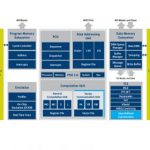
If you prefer a layered view of CEVA-Bluetooth solution, the above picture will help understanding the logical implementation and the various interfaces, from standard HCI to BlueRF-style RF interface, passing through (internal) APB processor interface.
Linley Mobile Presentation:
Ultra Low Power Integrated Platform for Connectivity and Audio/Voice/Sensing- Presentation
Eric Esteve from IPNEST
More Articles by Eric Esteve…..
lang: en_US