

My very first thought when hearing about HSPICE is using it for IC simulation at the transistor-level, however it can also be used to simulate a package or PCB interconnect very accurately, like in the PCB layout of a DDR3 system where timing is critical. I attended a webinar this morning that was jointly presented by Zuken and Synopsys entitled: Eliminate DDR3 Timing Errors with HSPICE and Zuken Constraint-based PCB Routing.
The two speakers were Griff Derryberry of Zuken, and Hany Elhak of Synopsys. The last time that I saw Griff he was attending an HSPICE SIG event in San Jose. I blogged about Hany back in February: Modeling TSV, IBIS-AMI and SERDES with HSPICE.

Griff Derryberry, Zuken

Hany Elhak, Synopsys
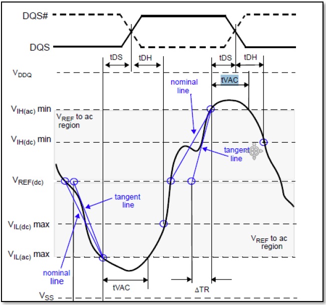
Designing a DDR3 system requires that you meet the multi-gigabit/second data rates while taking into account signal integrity issues, because the waveforms begin to look like deformed sine waves. The critical timing measurements are shown below: tVAC, tDS (setup), tDH (hold), tR (ringback)
The placement and routing of each DRAM package directly impacts the performance, so you need to do matched routing on the differential clock pair, and limit multiple route lengths.
Live Demo
Griff presented a live demo to show the steps used in the design and PCB layout of a DDR3 system. He used the following five EDA tools:
- Schematic Capture (Zuken)
- Constraint Manager (Zuken)
- Place and route editor (Zuken)
- HSPICE circuit simulation (Synopsys)
- Waveform results (Synopsys)
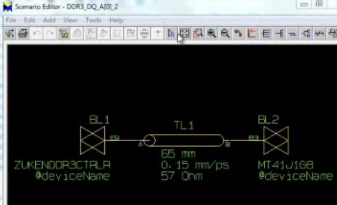
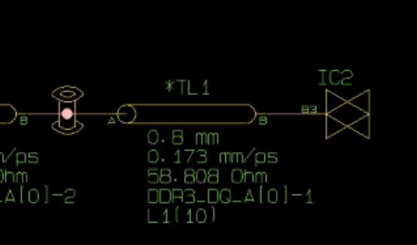
The schematic capture for the DDR3 system was done in a Zuken tool:
The memory controller is on the far left side, and the DRAM chips are in the middle. The first simulation was using an ideal transmission line, without actual PCB parasitics:
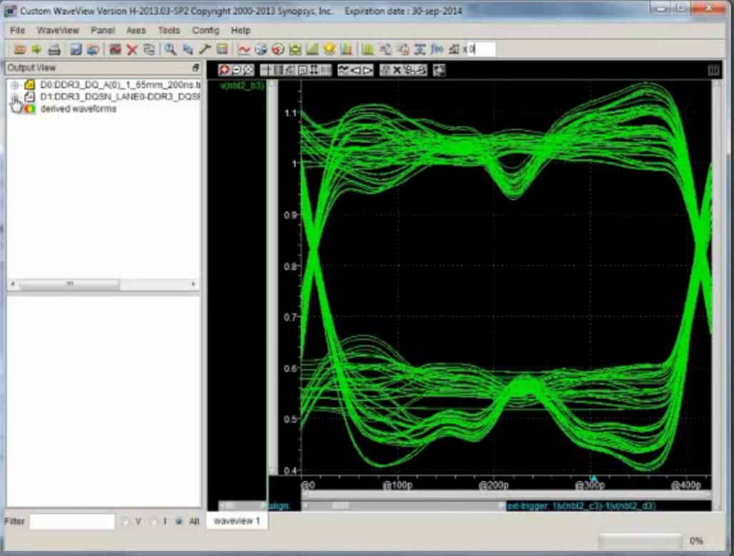
The eye diagram looks pretty good at this very early stage when viewing HSPICE results in Custom WaveTool, showing an aperture of 360ps:
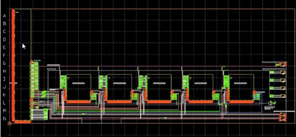
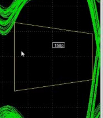
The next step was to do a quick placement and routing, then get a netlist with interconnect effects:
Now when this is simulated and measured there is an aperture of just 158ps, and several constraints were not met for tVAC, tDS, tDH, tR.
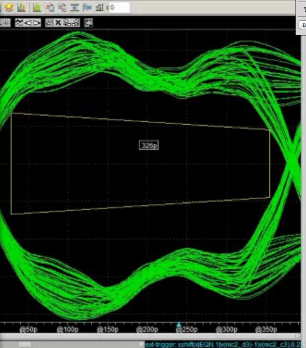
The final step was to change the routing, and this time using constraints to drive it. The requirement of 1.270mm maximum skew was met at 1.15mm by adding meanders to the routing:

With the new routing a netlist was extracted, HSPICE run, and results compared in the viewer showing an aperture of 326ps and no timing violations:
Q&A
Q: How do you control skew in the constraint manager?
A: We use the Constraint Manager for any of our nets, making a set.
Q: What simulation model did you use for traces on the board?
A: We know the traces, stacks, dielectrics, etc. It all gets extracted into the W element in HSPICE.
Q: What were the derating values?
A: The derating values are automatically loaded into Custom WaveView for you.
Summary
The methodology presented in this webinar shows that you can realize a DDR3 design and meet all the tight timing requirements by using constraint management, controlling the physical design placement/routing, and performing signal integrity analysis. EDA tools from both Zuken and Synopsys were used. To see the complete 33 minute webinar, view it here.
lang: en_US


Comments
There are no comments yet.
You must register or log in to view/post comments.