Since a few years, I have been following up Ansys Apachetools for semiconductor design, verification and sign-off. RedHawk is the most prominent platform of tools from Ansys, specifically for Power, Noise and Reliability Sign-off. It has witnessed many open endorsements from several of Ansyscustomers through open presentations, about which I have talked in the past. For a product, what can be a better promotion than its users speaking out for it? This is a win-win situation where a product earns revenue by satisfying its customers’ needs and in turn utilizes that revenue in enhancing it further to satisfy new needs of its customers, i.e. continuous improvement. One doesn’t need to go, acquire something new from the market to satisfy those needs. This philosophy is truly reflected in RedHawk’s development as I see it since last few years.
While RedHawk has been leading in the power, noise and reliability sign-off space since long, last year Ansys added significant capabilities into RedHawk by improving its capacity and performance to handle large designs with billions of transistors at sub-20nm and at very high clock speed of the order of 3+ GHz. That was a fourth generation release (with product named as RedHawk[SUP]TM[/SUP]-3DX), right in time when customers needed it. A great extension for 3D-ICs was provided which supported both concurrent and model-based multi-die simulations of designs with silicon interposer and TSVs. While simulation of all chips could be done at full layout detail, model-based approach allowed CPM[SUP]TM[/SUP](Chip Power Model) for some of the chips. A multi-tab, multi-pane GUI was provided to view and analyze voltage drop hotspots and other characteristic in the whole 3D stack at once. The sign-off accuracy and coverage was enhanced with the use of new event and state propagation engines that could be used in vector-based, VectorLess[SUP]TM[/SUP] and mixed-excitation modes, to gain maximum coverage without loss of accuracy.
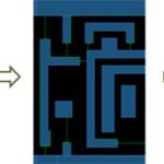
This month, Ansys announced RedHawk 2014 platform which supports FinFET-based semiconductor design (along with all earlier process technology based designs). As FinFET-based designs working at low operating voltages exhibit lower noise and reliability margins, greater emphasis has been provided on accuracy of analysis. The platform has been added with ‘Distributed Machine Processing’ (DMP) capability which improves memory footprint and simulation runtime each by about 2-3x over its previous release and handles large designs of the order of billions of transistors at flat simulation accuracy.
RedHawk-CPA is another great and unique capability in the 2014 platform which provides chip-package co-simulation and co-analysis. This is done by merging a fully distributed package parasitic network with an on-die power delivery network, thus allowing the tool to provide immediate feedback on the quality of the package design as well as the impact of package parasitic on the chip performance.
A testimony of RedHawk 2014 handling tighter EM (electromigration) limits and new EM rules (such as those considering current direction, metal topology and via types for power as well as signal nets) posed by FinFETs is its certification by TSMC. In order to counter heat reliability issue, a novel concept of CTM (Chip Thermal Model) has been introduced which can very accurately capture the thermal distribution for FinFET devices and enable a thermal-aware EM analysis.
Also, ESD integrity, an important step in reliability has been enhanced by careful ESD design planning to check degraded diode protection and reduced wire capacity.
While looking at Ansys’s agenda in DACwhere they will provide more detailed views and information about this new release of RedHawk 2014 platform, I observed several of their customer presentations scheduled at DAC where the actual users of these tools will be speaking about how they were benefited from RedHawk and other tools of Ansys. It will be interesting to closely watch those presentations to know about the real value of these new enhancements in RedHawk, at least RedHawk-3DX. Of course, a few of them, if they would have used customer beta version of RedHawk 2014, may reveal about that as well.
Here are some of the important customers I noted who would primarily talk about their experience with RedHawk, results and recommendations –
Jun 2, 1:00 PM – Samsung: Chip-Package-System based Power Integrity Analysis Flow for 14nm Mobile Designs
Jun3, 3:00 PM – NXP: Noise Coupling Analysis for Advanced Mixed-Signal Automotive ICs
Jun 4, 12:00 PM – STMicroelectronics: Designing Smart Power-Grid with Reduced Die-Area Using RedHawk
Jun 4, 1:00 PM – LSI: Silicon Correlation of RedHawk Dynamic Voltage Drop in High Power SoC for Storage Application
There are other interesting presentations by Applied Micro, Cienaand Synapse. Also, there are product specific sessions and multiple other customer presentations at various locations within DAC premises. Look at the Ansys page here for more details.
Registerfor any of these presentations. Ansys is exhibiting at booth #1413, it will be worthwhile to pass through that. Stay tuned to hear from me on details of some of these interesting presentations at a later date.
More Articles by Pawan Fangaria…..
lang: en_US