webinar IPXACT banner

Sidense overlays OTP on TSMC 16nm FinFET

Sidense overlays OTP on TSMC 16nm FinFET
by Don Dingee on 09-13-2014 at 7:00 am

Process shrinks, which have served us well for most of the Moore’s Law journey, are reaching their limits. For switching transistors, the biggest problems of leakage current and gate oxide vulnerability in planar MOSFETs have led the industry to new 3D microstructures such as FinFET. For non-volatile memory, the problem is generally not speed, but endurance and reliability.

In flash memory, smaller cells are more vulnerable to wear when subjected to repeated write operations, and more susceptible to corruption related to noise from nearby cells under programming and other sources. To combat this, 3D V-NAND flash technology has moved to a cylindrical structure, stacking layers of flash cells vertically and relaxing the geometry from 1Xnm class back to 3Xnm class. This effectively packs more cells in the same die footprint, simultaneously relieving the pressure on smaller geometry cells that adversely affects endurance.

Discrete NAND flash is usually fabricated in its own bulk process with dedicated design rules, not a luxury in SoC design (barring stacked 3D substrates, which would still be costly). There have been significant advances in embedded NOR flash at larger geometries, but there are still problems at 1Xnm with respect to write endurance. The dawn of FinFET also brings the challenge of how to cost-effectively fabricate embedded flash structures; lots of research, little commercialization yet.

This makes the reflex to “just grab some flash” a bit problematic for SoC designers adopting FinFET processes right now. Fortunately, many use cases for non-volatile storage can be implemented with one-time programmable (OTP) memory. OTP doesn’t have the same write endurance consideration since each cell is only written once. It fits where the need is for a relatively small but very important space to store encryption keys, tuning parameters, and other information.

To be cost-effective, OTP should live within the confines of the process for the SoC it resides in, ideally requiring no additional process steps for implementation. Overhanging concerns with reliability naturally exist at smaller geometries, and OTP is no exception – but the right approach could manage those issues.

With that in mind, Sidense has announced a very significant breakthrough: a demonstration of OTP cells in TSMC 16nm FinFET. Initial reports are impressive: correct bit-cell operation, using a programming voltage comparable to Sidense 1T OTP in 28nm, with a 10x lower leakage current. Additionally, margins between programmed and unprogrammed cells and post-bake cell stability both appear on target.

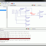
How was this, which Sidense believes to be the first working antifuse OTP in FinFET, accomplished? Sidense shared the following diagram (but few details) exclusively with SemiWiki:


This shows how Sidense is leveraging the 3D nature of the FinFET to implement the bit cell, with “no extra steps to the process” quoting an unnamed R&D source. We didn’t get too far with inquiries for specifics, but respect that the technology is still in development and details may be patentable and changing. We do know that TSMC has done extensive work in aligning overlays on FinFETs, and is likely deeply partnered in this Sidense research.

Initial functional and reliability testing of the OTP implementation in 16nm FinFET gave Sidense and TSMC enough confidence to announce the progress, a good sign for SoC designers. This is a development to watch carefully.

Related articles:
FinFETs for your next SoC


Expert Tool to View and Debug Design Issues at Spice Level

Expert Tool to View and Debug Design Issues at Spice Level
by Pawan Fangaria on 09-12-2014 at 7:00 am

Spice view of a design, block or fragment of the design is probably the lowest level of functional description of a circuit in terms of transistors, resistors, capacitors, interconnect and so on, which in several ways acts as an ultimate proof of pudding for any semiconductor design before manufacturing. However, it’s generally very clumsy and difficult, unless one is an expert Spice level engineer, to read and understand a design description (which may be a basic library cell) written in Spice. Not to mention, Spice levels circuits (which could be in the form of library cells) are integral part of digital, analog, mixed-signal, PCB and even MEMS designs. And it’s not possible to have large designs directly in Spice format; that’s the reason often a need arises to look at a small portion of design in Spice format. What if we have an automatic tool which can generate circuit schematic on-the-fly at any desired level of hierarchy, show multiple views in different windows including Spice source code to cross probe among them and several other features for easy debugging of a design at Spice level? I guess that will be an ultimate in getting us closer to that proof of pudding.

Although I have talked about several capabilities of Concept Engineeringaiding into SoC design, debug and verification, I realized the real value of SpiceVision PRO when I looked at its capabilities in detail and also watched a quick demo videodedicated to SpiceVision. It’s a must see to appreciate the real power of the tool.

SpiceVision provides a graphical Spice netlist viewer and analyzer for pre-layout as well as post-layout Spice including parasitic netlist in SPEF, DSPF or RSPF format. It supports 32-bit as well as 64-bit database to accommodate large SoCs. It also provides Tcl based userware API interface which can be used for advanced customization and electrical rule checks (ERC). The interface allows access to the internal database and GUI, through which users can analyze the design data and generate specific reports and design checks as desired. Selected fragments of circuit and critical paths can be easily and clearly displayed through a Cone Window feature. A circuit fragment can also be saved as a separate Spice file which can be simulated and debugged later. There is provision to export schematics into CadenceVirtuoso Schematic Editor Environment.

The design can be viewed at all possible hierarchy levels from top level to all sub-circuit levels. The hierarchy tree, source code and schematic diagram are displayed in different adjacent windows. A search engine can be used to generate a list of interest entities from which the designer can select any portion to generate the circuit diagram.

Any selected fragment or critical path can be displayed in magnified form in a Cone Window and details (such as R, C, and transistors) viewed and analyzed. The fragmented portion of the circuit can be exported as Spice netlist for partial simulation which can run 10 to 100 times faster compared to full circuit simulation.

At times, when a circuit become too much cluttered due to detailed display of parasitics, it becomes very difficult to recognize the actual circuit. SpiceVision has a feature where parasitics such as parallel capacitors can be merged to simplify the circuit. Also, the circuit can be displayed with just transistors or gates without parasitics, thus enabling designers for further design navigation and exploration.

As a final validation of the circuit, the layout at the final stage is extracted for verification which generates very large and complex SPEF and DSPF netlists with multiple critical paths. These critical paths can be displayed, analyzed and saved for critical path simulation. SpiceVision eases post-layout debugging significantly.

The specific part of a design saved in separate Spice file can also be used as IP in other designs. The symbols of components such as resistors, capacitors, transistors, current/voltage sources etc. are used as standard symbols, however they can easily link to external symbol libraries.

To get more information on this product, obtain the datasheet here.

More Articles by Pawan Fangaria…..


Transceiver Verification of a 20nm Altera FPGA Device

Transceiver Verification of a 20nm Altera FPGA Device
by Daniel Payne on 09-11-2014 at 6:00 pm

FPGA devices are a great way to drive silicon technology development because they contain both digital and analog IP, along with sophisticated IO cells. The highest performance IOs are transceivers, and Altera has recently designed the Arria 10 device family to include up to 96 transceivers, using a 20nm technology that can achieve data rates up to 28.1 Gbps. Users just know that there is a transmit and receive pair, however inside of the FPGA there are complex building blocks to sustain these data rates:


Arria 10 FPGA Transceiver Block Diagram

These transceiver cells are really analog IP that require transistor-level circuit verification and validation to work across:

  • Process corners
  • Operating voltages
  • Temperature ranges

Multiple clock sources are used in the transceiver block diagram, one of them is called fPLL, or Fractional-N Phase Locked Loop, and it provides both integer and fractional frequency clocks, with a range of data rates from 611 Mbps to 12.5 Gbps.


Fractional-N PLL

A traditional SPICE circuit simulator could be used to verify the proper operation of this sensitive design, however you would likely have to wait days to get results with a dynamic range greater than 100dB. To get simulation results faster you might even be tempted to use a FastSPICE simulator, however the results wouldn’t be accurate enough. Fortunately, there’s a happy medium between using a SPICE and FastSPICE circuit simulator, and that is using an Analog FastSPICEtool instead. Engineers at Berkeley Design Automation(now owned by Mentor Graphics) created this product category several years ago, and it has found a growing place in the family of transistor-level simulators where speed and analog accuracy are required.Related: Analog FastSPICE Update at DAC

Mentor has nicknamed their Analog FastSPICE tool AFS, and at Altera they were able to use AFS on transceiver simulations with up to 16M elements, which included post-layout netlists. Eye diagrams are a common analysis method to evaluate how clearly a sequence of 1-0 can be sent or received.


Transceiver Eye Diagram

At the 20nm node, a more rigorous validation and characterization flow was specified at Altera to include five metrics:

  • Systematic verification under all conditions, well-defined pass/fail criteria.
  • Automated regressions for pre-layout and post-layout netlists.
  • Ensure a common design environment and simulation conditions, consistency.
  • Uncover any statistical failing corners prior to tape-out.
  • Track all validation progress.

Within the Mentor EDA tools there’s something called the Analog Characterization Environment(ACE), and this was used to ensure that the five metrics listed above were actually adhered to and accomplished. Some 250 tests were defined in this validation suite, and there were over 6,000 simulations run, including Monte Carlo.Related: Analog FastSPICE AMS — Simple, Fast, nm-Accurate Mixed-Signal Verification

With this flow you can look at statistical results to help make design decisions. The probability of each iteration is displayed in chart format with Percentage on the Y-Axis and parameter (foundry process variation) on the X-Axis:


Voltage Regulator Monte Carlo Distribution

The statistical results on the voltage regulator show that the design is not centered yet between the two red line values of 1.09 and 1.11, so tweaking the transistor sizes is required for this design to be centered for maximum yield.

Two more Monte Carlo simulation results uncovered circuits that required more tuning to meet specifications:


Rx AC Peaking Monte Carlo Results


DC Offset Results for the Secure Digital block

With over 6,000 circuit simulations used in this characterization and verification flow, accurate results were delivered in a timely fashion by using AFS technology, like:

  • Multithreading
  • Multi-core parallel
  • Distributed multi-core parallel

Many of these runs could be automatically distributed across cores in a single machine, and across multiple machines. Managers and designers could look at the progress of verification across all the characterization variations.

Summary

20nm design is demanding, requiring a massive amount of circuit simulation to characterize and verify across: corners, sweeps, Monte Carlo and nests. Altera was successful in using Mentor tools like AFS and ACE in the design of their 20nm transceivers for the Arria 10 family.

There’s a six page white paper on this topic, ready for download after a brief registration step at Mentor’s web site.


Humans Need Not Apply!

Humans Need Not Apply!
by Daniel Nenni on 09-11-2014 at 7:00 am

With four children entering the job market I have a very simple piece of advice: DO NOT RUN FROM TECHNOLOGY, EMBRACE IT! Smartphones are now a “natural” part of modern life. We work on them, we play on them, we shop with them, we socialize with them, even risk our lives using them. Come on, every single person with a smartphone has used it while driving at least once. What’s coming next courtesy of our smartphone is rampant unemployment. Take a look at this clever video from C.P.G. Grey. It is well worth the 15 minutes:

This video isn’t about how automation is bad — rather that automation is inevitable. It’s a tool to produce abundance for little effort. We need to start thinking now about what to do when large sections of the population are unemployable — through no fault of their own. What to do in a future where, for most jobs, humans need not apply.

When I grew up, choosing a career was all about making money because as a family of 8 we did not have much to spare. Today I tell my children to choose a career they really, really enjoy because 30+ years is a long time to be doing it. So far I have a Math Teacher, a Fireman, a Mathematician, and a budding Marine Biologist and I couldn’t be prouder.

Fortunately for me, my teenage interests included electronics which brought me to computers then to semiconductors. Being in Northern California helped since Silicon Valley is where the fabless semiconductor ecosystem really began. I do remember however breaking the news to my family that I would do my undergraduate in computer science and receiving mixed reactions. Most notably was my Grandfather, a World War 1 veteran and bookkeeper by trade, who felt that computers would cause rampant unemployment akin to the Great Depression which he experienced firsthand. He lived to be 102 years old and I was his caregiver for the last 15 of those years so I heard some amazing stories, absolutely.

Going to the bank and the grocery store were two of his favorite outings and I remember when he saw his first ATM he honestly felt it was the beginning of the end. Scanners at the grocery store checkout were also not to be trusted so he would check his receipt like a bank statement. And he did find errors which pleased him on many different levels. Even today I sometimes find errors on my grocery receipt so that much has not changed.

Moving forward our smartphones will keep doing more for us, requiring less from us, and eliminating interactions with people on all professional levels. While I certainly do look forward to spending less time with doctors (health apps) and more time with new semiconductor based technology (IoT), I do wonder what stories I will tell my grandchildren. Given what we have accomplished in the last 30 years some of the stories will be hard for them to believe. Like the story my grandfather told me about delivering ice door-to-door every morning to make extra money. To his dying day his favorite “contraption” was the ice maker.


Smart Collaborative Design Reduces Business Risk

Smart Collaborative Design Reduces Business Risk
by Pawan Fangaria on 09-10-2014 at 4:00 pm

The semiconductor design industry is ever challenged with increasing chip density, manufacturing complexity with cutting-edge technologies, accommodating multiple IPs with different functionalities from various sources, optimizing power, performance and cost, maximizing manufacturability and reliability and still meeting ever shrinking time-to-market window with good quality and high yield. In such a diverse scenario of conflicting requirements, the business risk is going to only increase. And in the foreseeable future, this trend is going to continue and become harsher; semiconductor industry leaders have no other choice than assimilating diverse expertise and designing more tangled and complicated devices to differentiate and stay profitable in this highly competitive market. Unfortunately, the design tools and flows are also different (which is natural with diversity of expert solutions for particular problems), adding to divergence rather than convergence. So, what are the alternatives to move a design towards faster convergence?

Unity in diversity is the only mantra in such a situation where multiple teams work towards achieving diverse objectives of a design in a short span of time. The whole team has to be brought together (no matter how scattered or culturally different they are across the geography) on a common platform to achieve that common purpose of achieving design closure in the shortest possible time without diverting people from their set objectives. How’s that possible? Remember? I had talked about the “Design Collaboration Solution” in one of my blogon Dassault’sstrategy to move semiconductor design from productivity to profitability. What’s there in it?

Of course ENOVIA DesignSync has been there for managing large, distributed design data seamlessly from various EDA tools with hierarchical structure supporting IP assembly and re-use and host of other features to make data access efficient and protected through robust control mechanism. Another powerful capability enabling very effective and efficient collaboration among teams and leaders is ENOVIA Pinpoint. It provides graphical analysis of various parts of design, simulation results, test data, critical paths and other design specific data with dashboards for the whole team to take a shared view, assess timelines, identify the diverging paths and resolve by removing constraints or accelerating in particular directions. It provides great predictability in the design schedule and facilitates faster resolution of issues to achieve faster design closure.

ENOVIA Pinpoint by analyzing the diverse design data and bringing them together on a common simple visual dashboard for shared understanding between different tasks across design and verification evangelizes the teams and managers into pro-active thinking; communicating, finding and resolving problems (such as power, heat or timing) before they become critical. The data corresponding to any task can be accessed from central server through links and browsers and re-analyzed by respective design tools.

For accessing key data interactions to determine root causes, there is provision for ‘interactive plots’ and ‘configurable views’ to present the most critical data and analyze it to quickly identify outliers. The features include ‘Zoom and Pan’ to visually troubleshoot on the floorplan of the design from top to bottom in the hierarchy.

The ENOVIA Pinpoint solution provides multiple design factors such as timing, path and floorplan design which can be reviewed and improved. The floorplan can be superimposed with graphical results of various simulations such as critical paths and power hotspots which can help in taking decisions to improve the floorplan. Similarly, the reports such as ‘summary path data’ and ‘timing reports’ can be reviewed, bottlenecks in timing identified and re-design proposed to improve upon specific path delays.

The ENOVIA Pinpoint has a solid base of ~75 person-years of development and several years of use in semiconductor IC design and production. It’s a knowledge based tool in the sense that it brings attention to priority design issues and produces reports containing objective data, thus defusing tension between different teams or individuals, eliminating distractions due to useless (or subjective) data and keeping the teams focused on their common purpose. Also ENOVIA DesignSync has shown impressive improvements (20% – 74%) in various aspects of collaborative design such as production schedule, quality, IP re-use, multi-site design and productivity.

The Semiconductor Collaborative Design Process and tools from Dassault is being used by more than 120 IC design and development organizations around the world, which includes top 13 semiconductor companies. I love the words of Dwight Galbi of Qualcommwhen he says, “It’s as easy as Google Maps, as the tool zooms down to a single instance, which allows you to diagnose the particular problem. Then you can zoom all the way back out and map all of the failing paths and compare them to your layout.”

More on the Semiconductor Collaborative Design strategy from Dassault can be found in their eBook here. Stay tuned to get more updates on other parts of the entire strategy towards Silicon Thinking Industry Solution Experience.

More Articles by Pawan Fangaria…..


What’s eSilicon Up To Now?

What’s eSilicon Up To Now?
by Daniel Nenni on 09-10-2014 at 10:00 am

eSilicon, in conjunction with King Research, is conducting an unusual survey. A lot of vendor-driven surveys focus on specific pain points that are addressed by that particular vendor’s product/service. The idea is typically to either promote visibility for the product/service or establish its undeniable need in the market. eSilicon is a fabless ASIC provider, so I would expect their survey to focus on ASIC vendor issues.

This is not the case. The survey that eSilicon and King Research are conducting is far broader and more comprehensive than that. They touch on all kinds of design, manufacturing and operational challenges. You can check out the survey here. Paul McLellan also blogged about it recently. The survey title is also interesting: “Big Data, the Cloud and Internet of (Silicon) Things”. It seems to me eSilicon and King Research are up to something that is not typical for a fabless ASIC company. The collection of markets known as the Internet of Things will have a dramatic impact on our lives. The semiconductor industry will be impacted for certain – in a positive way for those who can see the trends. I recently shared the graphic below as part of my opening remarks at an eSilicon webinar on their GDSII quoting portal. The numbers are staggering:
eSilicon has been making noise about changing the industry using novel Internet technologies. We’ve seen some examples of that with their recent automated quoting portals. It’s interesting to note that these quoting portals have the potential to set a new bar regarding the value of Internet transactions. Again, from my opening remarks at the eSilicon webinar I shared this graphic:

The red circles show average transaction value for a few of the markets listed. Some people are buying their next car on the Internet, so that’s driving transaction value higher. But when we talk about semiconductor tapeouts over the Internet, those numbers get much, much larger. This trend for Internet transaction value is interesting, but eSilicon’s survey is also talking about Big Data and the Cloud. That suggests something else is going on. Something bigger.

I suggest you take their survey – let your voice be heard. eSilicon has done some pioneering work in the past and I think they are capable of more surprises, absolutely.

As a “thank you” eSilicon will be awarding $100 gift certificates from Amazon.com to five survey respondents. My beautiful wife and I shop Amazon all the time; we will weigh in on the survey, too. One last point – at the end of the survey you can volunteer to be part of a follow-up discussion. If you do that, you’re guaranteed an Amazon.com gift certificate. May the odds be ever in your favor…

About eSilicon
eSilicon, a leading independent semiconductor design and manufacturing solutions provider, delivers custom ICs and custom IP to OEMs, independent device manufacturers (IDMs), fabless semiconductor companies (FSCs) and wafer foundries through a fast, flexible, lower-risk, automated path to volume production. eSilicon serves a wide variety of markets including the communications, computer, consumer, industrial and medical segments. www.esilicon.com.


What Apple Talked About on 9/9/2014

What Apple Talked About on 9/9/2014
by Daniel Payne on 09-09-2014 at 5:00 pm

In America the popular press talks almost non-stop about: Disasters, politicians, celebrities and Apple. Yes, Apple. Today I watched the live cast of the new Apple product announcements.

iPhone 6
First, the see things differently video started playing, then the live stream died so I had to turn over to CNET where they were live commenting. 30 years ago the first Macintosh computer with iconic mouse-based graphical user interface, and bit-mapped graphics was announced at the Flint Center. Today we heard about the new iPhone 6 and iPhone 6 Plus, like rumored, in screen sizes at 4.7″ and 5.5″, catching up to the Samsung Galaxy Note introduced in 2011.

The A8 chip has 2 billion transistors, designed in the 20nm process node, and a 64 bit architecture. The M8 is the new motion chip which allows Apps to measure acceleration, count steps, stairs, altitude and barometric pressure. About 28 minutes into the announcement the Apple Live cast came back to life.Related: A Brief History of IC Design at Apple Computer

Usability improvements:

  • Voice over LTE (WiFi instead of cellular)
  • 8 megapixel camera, all new sensor, faster auto-focus
  • A8 chip with image processing built-in
  • Digital image stabilization (6)
  • Optical image stabilization (6+) – better than digital
  • Video at 1080p with 60 fps, slo-mo at 240 fps

Apple fanboys can wait in line on September 19th, or just go online to pre-order on September 12th.

iOS8

On the software side iOS8 comes out on September 17th across most iDevices. Justin Timberlake and Jimmy Fallon did celebrity promo videos for the iPhone 6 and 6+.Related: A Brief History of the Apple MacBook Pro

Apple Pay

Next up was how Apple is replacing physical credit cards with a new payment system called Apple Pay, based on Near Field Communication (NFC) technology. Android phones like the Samsung Galaxy S5 already use NFC for secure payments with the Google Wallet app. Expect to see Apply Pay launch next month and in a few dozen big-name retailers.

Apple Watch

One more thing…. As expected, we heard about the new Apple Watch, drawing a standing ovation from the crowd.

The strap is detachable, allowing users to customize the look to fit their own taste. The user interface is new, using the crown dial to select and navigate by clicking or turning. The display is sensitive to both touch and tapping, in a 3D sense. A taptic engine provides physical feedback. The custom-designed chip is called the S1, and complements the Taptic chip. Fitness metrics like heartbeat allow you to track health. You get three Apple Watch choices: Apple Watch, Apple Watch Sport, Apple Watch Edition. You’ll need an iPhone to operate your new Apple Watch (not stand-alone, or interoperable with anything else), and other features or apps include:

  • Siri, the voice-response system is built-in to Apple Watch.
  • Photo browsing
  • Text messaging
  • Maps with taptic response to turn left or right
  • Phone
  • Doodling
  • Fitness app – Heart beat
  • Workout app
  • Opening your hotel door at select venues
  • Find your BMW car
  • MLB sport scores
  • Honeywell home AC control
  • Apple Pay
  • Extendible platform for developers

Health and fitness was the final topic and Tim Cook talked about how the new Apple Watch gives you daily and workout feedback using technology like:

  • Accelerometer
  • Heart rate
  • GPS and WiFi (iPhone required)

Charging is required daily for the Apple Watch. This watch will cost you $349, and is available in 2015.

Summary

The new generation of iPhone 6 and 6+ are a step in the right direction, as Apple finally offers more than one screen size, following on the success of other consumer product competitors like Samsung and HTC. For me, bigger screen size is always better and I’ve been enjoying a 5.5″ display with my Galaxy Note and Note 2 devices for a few years now. The custom A8 and M8 chips make the iPhone 6 and 6+ possible, continuing the tradition of in-house, ARM-based design.

Apple Pay looks to be another promising merge of business deals and NFC technology to make retail purchasing easier. Apple Pay uses fewer keystrokes than Google Wallet on an Android phone to make a purchase, so that’s an improvement.

The Apple Watch isn’t first to market, but it certainly has the best marketing launch for a product in the wearable category, and I think that offering two different sizes makes more sense than one-size fits all. The $349 price makes this an instant, high-end, consumer status device. I look forward to learning more about the two custom chips inside of the Apple Watch family. As an Android phone user I am not compelled to buy an Apple Watch, and will continue to use my Cat Eye device to track cycling fitness.Related: IoT Application – Road Biking Fitness

Full Disclaimer: I do own shares of AAPL stock and use an iPad Air plus MacBook Pro each day.


Intel CEO Misinformed on the Foundry Business

Intel CEO Misinformed on the Foundry Business
by Daniel Nenni on 09-09-2014 at 7:00 am

At the Citi Global Technology Conference last week Intel (INTC) CEO Brian Krzanich made some comments about the foundry business that I found quite misinformed. It will be interesting to see if this theme is repeated during the foundry presentations at the Intel Developer Forum in San Francisco this week:

Intel is presenting two semiconductor manufacturing-focused sessions at the upcoming Intel Developer Forum that you may be interested in attending. By now you should have received instructions for complementary Intel Developer Forum registration, but please contact me if you have not and would like to attend IDF.

Leading at the Edge of Moore’s Law with Intel Custom Foundry
Speaker:Sunit Rikhi, Vice President, Technology and Manufacturing Group, General Manager, Intel Custom Foundry
Date/Time: Wed, Sept 10[SUP]th[/SUP], 4:00pm-5:00pm
Session Code: SPCS011
This session will provide an overview of Intel Custom Foundry’s capabilities and services covering a wide range of offerings including our silicon technologies, design platforms, manufacturing services including packaging, assembly and test capabilities. We will show you how Intel is unlocking the value of its Moore’s law leadership and its Integrated Device Manufacturing (IDM) strengths for the customers of Intel Custom Foundry. Topics include:foundry silicon technology offerings, design platform enablement, packaging and assembly, post silicon and manufacturing services, and eco-system capabilities.

Also Read: Intel Custom Foundry Explained!

Technology Insight: 14nm Process Technology – Opening New Horizons
Speaker: Mark Bohr, Intel Senior Fellow, Technology and Manufacturing Group, Director, Process Architecture and Integration
Date/Time: Wed, Sept 10[SUP]th[/SUP], 2:30-3:30pm
Session Code: SPCS010
Topics in this Technology Insight include:
• Transistor and interconnect features on Intel’s 14 nm process technology are described that provide industry-leading performance, power and density capabilities
• The 14 nm generation continues Moore’s Law in providing lower cost-per-transistor
• The 14 nm technology offers a rich mix-and-match feature set that enables a broad range of products from high performance server to low power mobile products
• 14 nm is Intel’s newest foundry technology offering, supported with a wide range of design tools

You can find the full IDF agenda here. I hope to see you at these sessions!

This is the misinformed quote I mentioned above:

“The relationship between the architecture and design guys and the silicon is important, because we really work together. This is the integrated device manufacturing advantage. We’re able to work together at a very early stage with a mutual target that says on this day we’ve got to have a product that has this cost and both sides have to bring this together to deliver that.

I think that’s the uniqueness that Intel has that makes it a little bit more difficult on the outside world. They kind of are handing something over a wall so to speak. And it’s just not quite as simple an integration.”

This is absolute nonsense. Handing things over the foundry wall stopped a long time ago. The fabless semiconductor ecosystem is today fully integrated into the foundry process development cycle, absolutely. This “early access” includes the top fabless semiconductor companies, EDA tool vendors, and IP companies. Look at how many of these companies have design and development centers in Asia. Do a quick LinkedIn search for ARM employees in Taiwan for example. Now try Synopsys and Qualcomm. Don’t bother with MediaTek because they are right across the street from UMC and TSMC. Hopefully this is just BK pandering to Wall Street because fabless semiconductor professionals certainly know better. Next time I hope an analyst asks BK what kind of early access Intel foundry customers have. :p

Also Read: What Does Intel Look Like 10 Years From Now?


A Comprehensive Power Analysis Solution for SoC+Package

A Comprehensive Power Analysis Solution for SoC+Package
by Pawan Fangaria on 09-08-2014 at 4:00 pm

Since power has become a critical factor in semiconductor chip design, the stress is towards decreasing supply voltage to reduce power consumption. However, the threshold voltage to switch devices cannot go down beyond a certain limit and these results in an extremely narrow margin for noise between the two. And that gets further challenged from increased variations in switching current and parasitics due to growing density and complexity of design in an SoC. Hence it becomes essential to analyze and optimize the complete power delivery network (PDN) of the system including the chip and package together to ensure reliable and stable voltage levels at all connection points of transistors. Amid minimum number of layers for package implementation and increased number of power domains in low power design arena, the package design plays a very important role (optimizing package impedance) in system design and must be considered together with the chip.

ANSYSRedHawk-CPA provides a comprehensive, accurate, fast and automated solution for any large system’s power integrity which accounts for L(di/dt) effects due to package inductance and decaps in its on-chip simulation. Its 3D FEM (finite element method) model based engine enables accurate extraction (high resolution per-bump distributed RLCK parasitics) of package layout for use in RedHawk simulation. The distributed modeling, which provides much finer pad voltage distribution than lumped model, enables accurate identification of weak pad placements that can lead to high dynamic voltage drop for instances in that region. RedHawk-CPA generates a broadband Spice netlist with ground parasitics and uses RedHawk to measure ground bounce separately, thus enabling net-by-net review of voltage drop and optimization of net geometries. Similarly, the package decaps enable instance-by-instance review of voltage drop, also taking into account the package decoupling, thus enabling optimization of package decap configuration.

The package layout (in any common format such as MCM, SIP or ODB++) can be directly imported into RedHawk-CPA and after its setup, the PLOC (bump location file) can be imported which is followed by automatic connections between package pins on the layout and bump locations on the chip without needing any designer to manually write connections in a text file in PLOC format, thus improving usability and productivity to a large extent. Of course, through an easy-to-use GUI, there is provision for a designer to override the automatic connections and do it manually as desired for particular connections. The voltage sources are assigned and the package model is generated that can be used seamlessly in RedHawk with GSR keyword ‘CPA_MODEL’, thus eliminating all designer written files including Spice wrapper with RLCK values of package instantiated under REDHAWK_PKG sub-circuit. RedHawk-CPA also allows designers to quickly perform static IR drop and AC hotspot analyses of the package layout following the RedHawk static and dynamic analyses respectively.

The high performance and capacity package extraction engine can easily handle large packages with quick turnaround time, allowing designers to quickly iterate over different chip-package designs and make important decisions such as bump placement early in the design cycle.

The RedHawk-CPA provides a very comprehensive report of design information, component Spice models, channel information, simulation control setup and results with maps and histograms that allow designers to easily review and visualize results.

The chip-package co-analysis provides simulations in both ways – package-aware chip simulation and chip-aware package simulation. The package DC IR simulation provides package static IR map which can be reviewed for current density violations on the PG nets of the package layout. The 3D FEM engine in RedHawk-CPA also allows designers to review AC hotspots on a given package layout based on the frequency content in the pad currents from RedHawk transient simulation. It allows a designer to review voltage/current maps/waveforms over the package layout/nodes over a desired frequency range. Near and far field EMI computations are also supported.

It’s a unique solution for chip-package co-design and analysis which is necessary to provide stable power delivery, reduce power consumption and maintain high reliability for today’s SoCs with high PPA factors. A further detailed description is provided in a whitepaperat ANSYS website.

I admire ANSYS also scheduling two separate sessions of free webinars where experts will provide practical level details on how to use RedHawk-CPA for chip-package co-analysis through its unified environment to perform DC, transient and AC power integrity analysis using chip and flip-chip package layouts to improve level of accuracy and shorten time to power closure –

Achieve Faster IC Power Closure Using Streamlined Chip-Package Co-Analysis

Tuesday, Sep 23, 2014 – 9:00 AM EDT, 1:00 PM GMT – Register here

Thursday, Sep 25, 2014 – 4:00 PM EDT, 8:00 PM GMT – Register here

These are very useful webinars to gain practical knowledge about system level issues with power and how to perform robust, accurate power integrity analysis and fix issues to design reliable SoCs.

More Articles by Pawan Fangaria…..


What Does Intel Look Like 10 Years From Now?

What Does Intel Look Like 10 Years From Now?
by Daniel Nenni on 09-08-2014 at 7:00 am

Intel (INTC) CEO Brian Krzanich keynoted the Citi Global Technology Conference last week. This was a precursor to the Intel Developer Forum in San Francisco this week. Normally these types of events are scripted dog and pony shows but sometimes interesting information comes out. The first question for example:

What does Intel look like 10 years from now?

According to BK, Intel will be a broader computing company with servers and personal computers worth more than $30B. Intel will be more mobile (pun intended) with wearables and Internet of Things. Clearly Intel has missed mobile and I highly doubt they will dominate wearables or IoT but since they own the really heavy boxes that we call cloud computing any investment in mobile devices will flood back to Intel.

On tablets, BK feels that Intel will be “fairly” successful going from 0% to probably 15% share this year. He’s talking about the Baytrail (22nm SoC) chip giveaway of course. 15% is a big number considering Intel is three to four years late to this market.

During the Intel analyst day presentations last November we learned that Intel would give away 40 million Baytrail SoCs to get traction in the tablet market even though BK told us before that Intel would SELL the 40 million parts. Intel called this “Contra Revenue” which is a clever term for a $1B+ write-off. Intel literally paid companies to take this chip. To me this SoC give away is a scorched earth strategy against the fabless semiconductor industry, specifically QCOM, Mediatek, Samsung, Apple, and the other mobile SoC companies.

The interesting thing to note, now that the AnandTech benchmarks are in, is that the 28nm Apple A7 is very competitive against the 22nm Baytrail which was billed as a generation ahead. Either the infamous Intel transistor domination slides do not apply to SoCs or, with SoCs, architecture is everything. In my opinion the answer is a bit of both. Apple will begin shipping the TSMC 20nm A8 this month and I can assure you it will run circles around any Baytrail based device, absolutely. My guess is that Intel will again have to contra revenue Broxton (14nm SoC) or cancel it all together.

Also Read: The Two Biggest Misses in Mobile

In regards to smartphones, BK admits Intel is still figuring out this market. Unfortunately, Intel is used to setting trends and not following them so smartphones above all will be a significant challenge. Right now Apple, Samsung, and Xiaomi are the mobile trendsetters and the competition is fierce. It was interesting that when BK was asked about competitive pressures he brought up AMD and how Intel dominated. I really think this is an apples to oranges comparison when talking about Qualcomm, Apple, and Mediatek. Intel was the leader and AMD the follower. Intel is now the follower in the SoC world and that is generally not a comfortable position for an established industry leader.

This however is the most interesting comment BK made:

“The relationship between the architecture and design guys and the silicon is important, because we really work together. This is the integrated device manufacturing advantage. We’re able to work together at a very early stage with a mutual target that says on this day we’ve got to have a product that has this cost and both sides have to bring this together to deliver that.

I think that’s the uniqueness that Intel has that makes it a little bit more difficult on the outside world. They kind of are handing something over a wall so to speak. And it’s just not quite as simple an integration.”

Quick question, how many of you leading edge fabless semiconductor professionals hand things over the foundry wall?

Also Read: Intel 14nm is NOT in Production Yet!