Semiwiki EDA Webinar 800x100

Join the Multi-die IC session on April 21 at EDPS 2016 in Monterey, CA

Join the Multi-die IC session on April 21 at EDPS 2016 in Monterey, CA
by Herb Reiter on 04-14-2016 at 12:00 pm

Following Moore’s Law down to 10 or even 7 nm labeled feature size demands US $ hundreds of millions of up-front investment, a very large design team and two or more years of development time. These parameters suggest that it only makes sense for very high volume applications to continue on the shrink path to increase SoCs’ functionalities.

However,
– how can you serve applications that don’t require a billion units over their life time and can’t pay back a large NRE?
– how can your company continue to grow if it needs to invest such large sums and “bet the farm” on a single project?
– how can you pack logic, memory, analog, RF, MEMS,… and other functions economically into a 7 nm SoC?

The Electronic Design Process Symposium (EDPS) 2016 will address these and many other questions on Thursday afternoon, April 21.

EDA, IC design and IC packaging experts will present their capabilities in support of packing multiple dies into one IC package, suggest where and how to combine multiple dies in a 2.5 or 3D-IC, or consider wafer-level packing. Half of the 2-hour session is reserved for discussing the benefits as well as answering your questions during the panel discussion.

Herb Reiter, from eda 2 asic, will introduce the session’s subject, outline his new consulting role at the Electronic System Design Alliance (formerly known as EDAC), highlight why our industry needs to complement continued shrinking with multi-die IC technologies, suggest what the represented industry segments need to do to further grow market acceptance of these innovations, introduce the panelists and also moderate the discussion with the audience.

Riko Radojcic, well known for his role as 3D-IC evangelist at Qualcomm, will share his vast expertise in how to determine cost advantages and technical reasons for choosing a multi-die IC technology for a specific application.

Mentor Graphic’s Dusan Petranovic will present and discuss the importance of accurate modeling and thorough verification for cost-effective and reliable multi-die ICs.

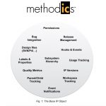
For companies who do not have sufficient in-house resources to execute a multi-die IC design and/or want expert advice for engaging the right supply chain partners, plan to develop a multi-die IC design methodology, want assistance to ramp up volume production for such ICs or other reasons, Design Services companies are ready and eager to offer their expertise. Asim Salim will represent Open Silicon, outline the team’s expertise and their important role in the Multi-die IC EcoSystem. See below the EcoSystem’s key segments and their individual roles.


The next speaker, Ivor Barber, has many years of experience in advanced IC packaging and will present why Xilinx chose to pioneer multi-die IC technology several years ago already. He’ll outline technical and business reasons for the success of Xilinx’ “Stacked Silicon Interposer Technology” (SSIT).

Paul Silvestri from Amkor, a leading IP Packaging and Test corporation, will show Amkor’s portfolio of traditional and recently introduced advanced IC packaging technologies, which include a very cost-effective family of Fan-Out Wafer-level packages.

After these brief presentations our experts will be available for an additional hour to answer questions from the audience. Herb will moderate this panel discussion and make sure that every attendee can see that the EcoSystem in support of multi-die ICs has made significant progress in the last few years. Now many partners can offer you viable products and services for your first (or next) multi-die IC design. You also can integrate one of your proven SoCs — in die-form — together with other die-level IP, such as a memory cube, in a multi-die IC package and enjoy the performance, power, form-factor and system cost benefits versus individual, fully packaged ICs on a PC board.

Just in case that you are still hesitant to fit EDPS into your busy schedule, click on the pointers below. The first one leads you to a recent article that describes how NXP/Freescale use their RCP interposer technology for a 77GHz automotive radar application: http://www.systemplus.fr/wp-content/uploads/2016/03/NXP_MR2001_Freescale_Radar-Chipset_Flyer_SPC_v2.pdf

The second pointer directs you to last week’s Nvidia announcement of the Tesla P100 GPU and their DGX-1 GPU server, utilizing four memory cubes surrounding a GPU on an interposer: http://www.eetimes.com/document.asp?doc_id=1329368

For many more articles about concrete applications of multi-die ICs and a lot of other information about the Multi-die IC EcoSystem, please click on this pointer and download the 324 page Multi-die IC Design Guide from the Electronic System Design Alliance’s website: http://www.esd-alliance.org/industry/publications

More about EDPS and other valuable sessions at: http://edpsieee.ieeesiliconvalley.org/edps_program.php

SemiWiki-EDPS2016promo code for a $50 savings.

See you at EDPS in Monterey next week….Herb


EDAC Name Changing for ESDA, but what about IP ?

EDAC Name Changing for ESDA, but what about IP ?
by Eric Esteve on 04-14-2016 at 7:00 am

The EDA Consortium (EDAC) has changed name for Electronic Systems Design Alliance (ESD Alliance). That’s a good reminder that IC are developed (thanks to Design Automation) to be integrated into a System. A wide design ecosystem support system development, including embedded software, design intellectual property (IP), embedded software, advanced packaging (3D, TSV,…) and design service companies.

Let’s focus on the design IP segment, which is now “officially” the largest category according with the results published by EDAC for Q4 2015 with $702.2 million and +9.2% growth (see the picture below).

I decide to focus on design IP for several reasons ; at first because we will see that the growing behavior of the segment monitored on a 20 years timeframe exhibit an amazing vitaly, almost imune to economical crisis. The second point justifying to look at the design IP business more carefully is that this segment is underestimated if you only look at EDAC results. Not because EDAC or ESDA doesn’t do a good job, but simply because the IP revenues reported quarterly by EDAC are generated by IP vendors being part of the organization. By definition, an IP vendor who is not an EDAC member will not report IP revenues to EDAC, and there is no way for EDAC to take these revenues into account.

Thanks to EDAC, we can monitor the revenues generated in the five categories by the members during the last 20 years, or 80 quarters. The dynamism of the Silicon IP (SIP, in clear blue) appears through the strong growth rate, SIP passing from (almost) zero in 1996 to $700 million per quarter in 2015. CAE, the former largest category, has grown from $300 to $650 million on the same timeframe. Or, if you prefer, it took only 5 years for SIP (2010 to 2015) to make a move which took 20 years to CAE (passing from 300 to 700).

Let’s zoom into the 2008 to 2011 period, covering the strongest economic crisis since 1929. SIP category has been impacted, strongly declining in 2009, like the other categories. But, it took only 5 quarters for SIP to come back to the pre-crisis level, when it took 10 or 15 quarters for CAE or IC Physical to recover. Why SIP has recovered much faster than tools categories?

Let’s take an example: a team is developing a SoC in 2009, and R&D cost has to be lowered due to the crisis. The project manager may decide to lower the EDA investment and buy 4 seat licenses instead of 6, for example. But if you need a GPU, or MIPI CSI PHY or PCIe PHY and Controller, taking the decision not to buy these IP and develop it in-house is possible, assuming you have the right design resource, but certainly a lot more risky than buying a Silicon proven IP to a vendor. We can assume that SIP is now a strategic piece of System-on-Chip development and IP outsourcing is clearly growing year after year, with 13% CAGR 2005 to 2015 as extracted from the above picture.

I have no problem with the data collected by EDAC as the result is representative of the IP business. When compared with data collected by IPnest for the Interface IP segment (in the $500 million for 2015) we observe the same growth and CAGR, as you can see on the above picture (issued in 2010, but the 2014 forecast fit with actual data with +/-4% error).

The problem with IP category from EDAC comes from the number of IP vendors reporting their revenue, as only five of them are EDAC members: ARM Ltd., Cadence, Sonics, Synopsys and Mentor Graphics. These five vendors have reported slightly less than $2 billion revenues coming from IP in 2015. It’s easy to guess that the total IP revenues have been higher, but the good question is how much higher.

I have built a non-exhaustive list of missing IP vendors, indicating their 2015 revenue when available from their annual report:

  • Rambus ($300M)
  • Imagination Technologies ($245M)
  • CEVA ($60M)
  • Faraday ($25M)
  • eMemory Technology
  • Kilopass Technology
  • Sidense
  • Aragio
  • Dolphin Technology
  • Andes Technology
  • Cortus
  • GUC
  • Arteris
  • Silicon Image
  • Arasan Chip Systems
  • PLDA
  • CAST
  • Northwest Logic
  • True Circuits
  • Mixel
  • Analog Bits
  • Silicon Creation
  • Silabtech
  • M31
  • Discretix
  • Sarnoff
  • Chips&Media
  • + several dozens

We can observe that four of them are reporting IP revenues for a total in excess of $630 million in 2015 ! I have listed another couple of dozens of IP vendors, either privatly owned, either reporting globally their revenue from IP, design services and NRE. If we assume an average revenue in the $10 million range for these companies, that makes $230 million to be added. If we consider that probably 30 to 50 companies are missing in the above list, we can evaluate the revenue generated by the IP business (not reported to EDAC) is most probably in excess of $1 billion… and this makes $3 billion in 2015.

In conclusion, the SIP category is certainly the most important of the chip design ecosystem, but the figures shared by ESD Alliance are underestimated, the real business figures being in the 40% to 50% higher. What could be done to correct this issue ? Maybe the ESD Alliance could launch a promotion campaign to convince the missing IP vendors to become ESDA members, offering a discounted subscription fee, as most of the missing companies are not as large as the current members… Beeing creative, we certainly could find other options to better know the real size of the Silicon IP market.

Whatever the selected solution, there is a real need to more accurately know the category which is now the most important in the chip design ecosystem !

Eric Esteve from IPNEST


Self-contained low power Wi-Fi IP for IoT apps

Self-contained low power Wi-Fi IP for IoT apps
by Don Dingee on 04-13-2016 at 4:00 pm

The emerging theme of fit-for-purpose IoT parts gained yet another perspective, this time with ARM and CEVA chiming in on a low-power Wi-Fi approach outlined in a new webinar. It was a rather unique event with an abbreviated 25-minute presentation and an extended 35-minute Q&A that added a lot of insight. Continue reading “Self-contained low power Wi-Fi IP for IoT apps”


Wearables Mean Continuous Growth in the Internet of Things Ecosystem

Wearables Mean Continuous Growth in the Internet of Things Ecosystem
by Bill McCabe on 04-13-2016 at 12:00 pm

The Internet of Things encompasses a wide range of connected services, technologies, and hardware devices. Yet, for consumers, it is the growing number of portable and wearable devices that will be their main interface with IOT tech. The wearable device market is rapidly evolving, especially when it comes to smart watches and fitness monitoring devices.
Continue reading “Wearables Mean Continuous Growth in the Internet of Things Ecosystem”


“Thinking Outside the Chip”

“Thinking Outside the Chip”
by Students@olemiss.edu on 04-13-2016 at 7:00 am

While pushing Moore’s Law’s boundaries in the world of 2D packaging, companies are starting to explore nontraditional approaches towards designing integrated circuit chips. 2D packaging is currently the most used method in designing chips in the industry, and while it leads in efficiency of power and performance, it lacks in the utilization of space which is always a concern in the chip industry. 2.5D and 3D packaging capitalizes on the use of space, which increases the capacity of chips to hold more transistors per unit area without an increase in the cross-area of the chip. With this advantage, 2.5D and 3D packaging have the potential to jump 2D packaging in the future.

Traditional 2D packaging predominantly refers to System-on-Chip (SoC) and System-in-Packages(SiP). SoC is a device that contains a package that holds one die that contains multiple functions. Due to having only one die, SoC demand low power to be used and has fast circuit operation; however, it is viewed that it is very difficult to design and alter. The whole SoC has to be replaced to add a function for the SoC to perform and a complete replacement is needed if a function does not work correctly. SiP contains one wafer that is connected to multiple individual dice by flip-chip bumps which are essentially solder bumps. The multiple individual dice are on the same wafer. Unlike SoC, SiP are flexible to be altered since they contain individual dice for different functions. The speed of SiP is slower than SoC due to more connections from the individual dice, which increases the chances for failing.

2.5D packaging is very similar to 2D packaging, except that 2.5D packaging uses a silicon interposer to connect the dice to the wafer. Silicon interposer contains a substrate that has metallic components on the sides. It uses through-silicon vias(TSVs) as tunnels to connect metallic sides of the silicon interposer. The dice are connected to the interposer with micro-bumps instead of the larger flip-chip bumps, and the silicon interposer is connected to the substrate with flip-chip bumps. Since TSVs use direct connections, 2.5D use less power to communicate with different components. The silicon interposer also limits the space needed for the use of rails. Adding the silicon interposer introduces additional cost and difficulty to designing and testing.

3D packaging involves the use of multiple dice stacked on top of each other using TSVs to connect the individual dice and the wafer. By using TSVs, the dice are able to interact with each other and the wafer. Due to the thin nature of the TSVs used, 3D packaging utilizes efficient use of space that is used to increase the capacity of the chip for containing more transistors per unit area compared to 2D packaging. The use of TSVs also leads to efficient communications between the die and better performance in terms of power since less power is needed for transmitting signals. Due to dice being stacked upon each other, heat dissipation is one of the major issues with 3D packaging. When the dice are stacked, high temperatures can cause the dice to melt. Additional problems involve the cost of testing since all current chip testing mechanisms are for 2D. The additional costs involved will lead to an increase in the price of the chips which will be divergence from the long trend of cost reduction in the chip industry.

Even though the 2D packaging is the main design being used in manufacturing, the 2.5D and 3D will eventually pass 2D packaging. The boundaries of Moore’s Law dealing with 2D packaging will soon be reached; therefore, 2.5D and 3D will be the future to increasing the amount of transistors per area. Since 3D packaging incorporates more dice per cross-area than 2D packaging, 3D will be the main leader for designs in the future. Despite the performance enhancements that these new packaging approaches bring, there are economic, and technical challenges that need to be navigated through before wide scale implementation in the market.

The economic challenges come from the added costs involved in making these new designs. The new designs involve die integration which costs more. The current existing testing structures are not suitable for the new designs. Although 2.5D design can use most of the existing 2D testing structures, 3D will require a complete overhaul which will be an added cost to the chip industry. The additional production cost will translate into higher prices for chips which is against the tradition of producing cheaper chips in the chip industry.[4] Since the dies are stacked upon each other, heat dissipation, which will causes the dices to melt, is a main issue. Until companies develop a new design that deals with the heat and the rising production costs involved, 3D packaging will continue to lag behind 2D and 2.5D packaging.

By Demba Komma and James Grantham

Article in question for reference:
[1]Sperling, Ed. “Thinking Outside The Chip.” Semiconductor Engineering. N.p., 14 Jan. 2016. Web. 23 Feb. 2016. .

References:
[2]Santarini, Mike. “2.5D ICs Are More than a Stepping Stone to 3D ICs | EE Times.” EETimes. N.p., 27 Mar. 2012. Web. 19 Feb. 2016. <http://www.eetimes.com/document.asp?doc_id=1279514>.
[3] Maxfield, Clive. “2D vs. 2.5D vs. 3D ICs 101 | EE Times.” EETimes. N.p., 8 Apr. 2012. Web. 19 Feb. 2016. .
[4]Bailey, Brian. “When Will 2.5D Cut Costs?” Semiconductor Engineering. N.p., 7 Aug. 2014. Web. 19 Feb. 2016. <http://semiengineering.com/will-2-5d-reduce-costs/>.


EUV is coming but will we need it?

EUV is coming but will we need it?
by Scotten Jones on 04-12-2016 at 4:00 pm

I have written multiple articles about this year’s SPIE Advanced Lithography Conference describing all of the progress EUV has made in the last year. Source power is improving, photoresists are getting faster, prototype pellicles are in testing, multiple sites around the world are exposing wafers by the thousands and more. The current thinking is that EUV will be ready for production around 2018. All of this is very promising but while we have been waiting for EUV the industry has been moving on and a possible scenario is emerging where by the time EUV is available it won’t be very useful. In the balance of this article I will lay out a possible scenario where changes in device structures and fabrication processes could make EUV largely unnecessary.

My Advanced Lithography Articles summarizing the recent progress of EUV are available here:

There are three major product categories that drive capital equipment purchases in the semiconductor industry today, NAND Flash, DRAM and Logic.

For many years NAND Flash drove the requirement for the latest lithography tools. 2D NAND Flash devices went through lithography shrinks yearly eventually reaching 16nm devices manufactured in high volume with Self Aligned Quadruple Patterning (SAQP), but difficulties with 2D NAND device scaling and the cost of the complex patterning schemes required have brought 2D NAND scaling to an end. Specifically, adjacent cell interference, control to floating gate coupling and the shrinking number of electrons in a cell are just some of the device related issues. The solution to this issue for NAND has been the move to 3D. 3D NAND creates strings of NAND cells vertically with the cells created by alternating layers of material deposited using CVD techniques. The lithography requirements for 3D NAND are relaxed, for example Samsung’s 32-layer part has only one double patterned layer. Scaling is accomplished by adding layers, not by shrinking the photolithography defined dimensions. It is expected that scaling to >100 layers will yield devices with over 1Tb of capacity. 3D NAND has therefore made EUV unnecessary for NAND.

DRAM has followed a path similar to 2D NAND with yearly shrinks and the use of complex multi-patterning schemes. Recently DRAM scaling has slowed due to device scaling issues. DRAM stores values as a charge or absence of charge on a capacitor fabricated in series with an access transistor that controls the capacitor. Access transistors need a relatively long channel length to minimize leakage. This has led to a variety of access transistor structures such as RCAT, SRCAT and Saddle fin. The next step in access transistor scaling is expected to be VCAT but to-date fabrication of the vertical VCAT has been difficult to achieve. In parallel to this the DRAM capacitors need to scale down in horizontal area while maintaining a minimum acceptable capacitance value. Capacitor scaling to-date has involved vertical structures, rough surfaces and high-k dielectrics. Further vertical scaling has been limited by mechanical issues. and there is also a fundamental trade-off between the dielectric constant (k) of a material and band gap. As k increases the band gap decreases leading to leakage problems. Achieving acceptable leakage through the capacitor constrains the materials that can be used. There are some options still available, for example bit line optimization may allow smaller capacitance values to be used and there are rumors of a new film. At present the device scaling issues have moved DRAM away from being a leading candidate for EUV usage. DRAM also appears to be a leading area of Directed Self Assembly (DSA) research.

Longer term a DRAM alternative is needed. Conventional wisdom is that STT MRAM will eventually replace DRAM. To-date MRAM density and therefore cost is not competitive with DRAM (and there are other developmental issues). MRAM cells are fabricated in the metal layers over logic devices opening up the possibility to move to some kind of 3D Structure, possibly similar to the recently disclosed 3D XPoint memory (more on that later).

In the logic space the leading companies, Intel, TSMC, Samsung and Global Foundries are all in production of 16nm/14nm FinFETs. 10nm is expected to start to enter use in late 2016 at the foundries and in late 2017 at Intel. TSMC is currently forecasting that 7nm will be available in late 2017. TSMC is guiding that they will “exercise” EUV at 10nm for 5nm use. Intel is leaving the door open on EUV use at 7nm and assuming they don’t produce 7nm until 2019 or later that would make sense. Global Foundries has said they are developing 7nm based on what they can reasonably do without EUV and EUV would be a possible second generation 7nm cost reduction. All of this lines EUV up for a projected late 7nm node or 5nm node insertion.

Against this backdrop it is interesting to look at the evolution of logic devices. Intel introduced FinFETs at 22nm, shrunk them for their second generation at 14nm and they are guiding that at 10nm the third generation FinFETs will not have new materials. 16nm/14nm at the foundries was the first generation FinFET for all of them, 10nm will be the second generation and 7nm the third generation FinFETs for them (we should note here that from a pitch perspective the foundries 7nm “node” is similar to Intel’s 10nm node). At one time I thought we might start to see FinFETs with high mobility channels by 7nm or possibly even 10nm but due to a variety of challenges achieving high performance with high mobility channels in actual devices and the challenge of changing an existing structure to a new material I am now thinking FinFETs will likely stay with silicon channels until they are replaced by a new device. This leads to the question of when we might see a new devices and what it might look like.

IMEC is one of, if not the leading semiconductor technology research institution in the world. IMEC appears to be settling in on stacked horizontal nanowires as the successor to FinFETs. The devices experts I talk to are also optimistic on this approach. Horizontal nanowires are fabricated by depositing a stack of alternating materials using CVD techniques and then pattering them. This technique can create a stack of multiple nanowires. One really intriguing possibility is for example to create a 4 nanowire stack where 2 wires are NMOS and 2 are PMOS. This would yield a stacked CMOS devices and be equivalent to a node or more of scaling without shrinking the lithographic dimensions. If you take this idea a step further to 8 stacked wires you could have a stack of two CMOS pairs. You could also look at stacking layers while relaxing the horizontal width to scale the device density while taking the pressure off of lithography to provide shrinks. This would be analogous to what has been done with 3D NAND.

Of course we also need to look at when this might happen. My best guess is around 5nm at least for the foundries. With the foundries lining up to not use EUV at 7nm or only late in 7nm, if a 5nm solution emerges that doesn’t need EUV how much of a EUV investment are they likely to make. For Intel I am thinking horizontal nanowires might be a 7nm solution but with Intel now on a 3-year node cadence that would put Intel’s 7nm node at around 2020 likely around when the foundries would be introducing their 5nm nodes.

The picture all this paints is that NAND no longer drives the need for EUV by going to a 3D structure and logic also has the potential to move to a 3D structure with relaxed requirements. DRAM scaling has slowed due to device scaling issues and is a leading DSA candidate, so what will drive the need for EUV?

Intel and Micron recently introduced their 3D XPoint memory architecture. Faster and with better endurance than NAND and cheaper than DRAM, 3D XPoint is positioned to be used as Storage Class Memory – a kind of buffer between DRAM main memory and non-volatile storage such as NAND and hard disc drives. The first 3D XPoint memory has 2 memory layers fabricated in the interconnect stack over a logic circuit that controls the memory. We estimate the memory layers take 2 mask layers each and are a 25nm technology requiring multipattering for each layer. 3D XPoint scaling offers the ability to scale by adding layers and also by shrinking the memory layer pitch. If 3D XPoint is scaled simply by adding memory layers EUV might not be interesting. If 3D XPoint were to begin scaling pitch, EUV would become attractive. With 3D XPoint not expected to be in production until 2017 and then needing to become established in the market it is hard to envision 3D XPoint successfully driving EUV adoption.

This is of course just one possible scenario for the direction of semiconductor technology but clearly while we have been waiting for EUV the industry has been moving forward on other fronts. Multipattering also continues to get better and cheaper. By 2018 when EUV is currently projected to be ready for production it is possible the evolution of semiconductor devices may make it unnecessary.


Making PLM Actually Work for for IC Design

Making PLM Actually Work for for IC Design
by Tom Simon on 04-12-2016 at 12:00 pm

The topic of Product Lifecycle Management (PLM) conjures up images of usage on airplanes, tanks and cars. That’s because it was developed decades ago to help make product development and delivery more efficient for big expensive manufactured products. It worked well for its intended markets by combining and managing all the phases of product development, parts procurement and manufacture. Unfortunately, while the concept is sound, there has been little feasible success implementing classic PLM systems for IC design.

There are several significant reasons that PLM has not gained traction in the IC design space. Traditionally PLM systems are applied by taking a relatively static design and manufacturing process and building an extensive set of customizations and specially tailored code to handle that one specific case. As we know IC design is changing at every node, and even at existing nodes, flows and tools always being updated. As a result, rather than setting up a system and using it continuously, IC design requires adaptability in PLM systems.

Another big difference in IC design is how semiconductor IP’s are really hierarchically self contained designs themselves. So rather than taking a flat bill of materials from suppliers or internal sources and assembling them in to a finished product, IC’s have layer upon layer of blocks that are each themselves potentially composed of smaller IP blocks. The requirement for semiconductor PLM’s is to manage all the design and verification steps at each level as information is moved from development to utilization.

The data we are talking about includes technology files, tool versions, quality metrics, constraints specifications, dependencies, etc. Also access control and release management, and a number of other features are necessary. In fact, Methodics has compiled a list of all the properties that are needed in each base object in an IP PLM system.

Methodics is well versed on this topic because they have developed a PLM system specifically tailored to semiconductor design. It uses their ProjectIC design management system as its foundation. In turn ProjectIC is built upon industry standard revision control systems such as Perforce, GIT or Subersion, used in their native form. The real question, however, is what are the steps to connect Methodics’ IP Lifecycle Management (IPLM) system to a semiconductor design project and all of its potentially hierarchical IP components.

Fortunately, Methodics has written up a white paper that covers the fundamentals and also the integration points for their IPLM system. The process starts with customers adding in meta data for the IP that they wish to include. This can be run as a batch operation once the specific fields desired have been defined. There is some discretion here as to what to include, but the flexibility allows customers to attach whatever metadata they deem important for each IP block. It is also easy to update or modify these definitions.

Next is the process of importing existing IP into workspaces so they can be worked on and released to other users and teams. Now, IP can be changed and worked on in a systematic fashion. Also any tool run results can be captured and saved. This might include P&R results, or the output from verification runs such as DRC, simulation, etc. All this information is maintained with the IP for future reference and use.

At this point it is possible using Methodics’ IPLM system to create releases for the IP users who depend on the IP. As downstream users integrate these IP releases into their own designs, data about where the IP is used is saved. This means that it is possible to determine where specific IP is used.

Other metadata can be added back into the IPLM system from downstream users and external sources. Custom metadata can be created using the ProjectIC API’s. These comprehensive API’s are well documented and make it easy to create custom scripts to provide richer data on IP implementation and deployment within an enterprise.

The Methodics white paper goes into much deeper detail than we have space for here. If you are interested in how PLM can realistically be applied to semiconductor design, reading it is highly recommended. A copy is available through their website.


2.5D supply chain takes HBM over the wall

2.5D supply chain takes HBM over the wall
by Don Dingee on 04-11-2016 at 4:00 pm

SoC designers have hit the memory wall head on. Although most SoCs address a relatively small memory capacity compared with PC and server chips, memory power consumption and bandwidth are struggling to keep up with processing and content expectations. A recent webinar looks at HBM as a possible solution.
Continue reading “2.5D supply chain takes HBM over the wall”


Neural Networks Poised to Make Big Changes in Our World

Neural Networks Poised to Make Big Changes in Our World
by Tom Simon on 04-11-2016 at 12:00 pm

Probably the most interesting thing about Neural Networks is how they can be used for complex recognition tasks that we as people can easily perform but we might have a lot of trouble explaining how. One very good example of a problem that Neural Networks can tackle is determining when people are making a fake smile. Intuitively we know how to do this, but we would be hard pressed to explain the process we use to do it.

Neural Networks are being used for facial recognition, medical diagnosis, autonomous vehicles, and more. The list of applications is limitless, and the best part is that problems can be thrown at Neural Networks without having to map out a specific solution. Instead of hard coded programs that can do one specific task and no other, we can build a Neural Network and train it over and over again to do whatever tasks we want it to perform.

The power and potential of Neural Networks has not gone unnoticed by the major players in software and hardware. At the CDNLive event in Silicon Valley last week, Cadence CEO Lip-Bu Tan’s keynote talk featured Neural Networks. A few months ago Cadence hosted an event specifically targeted at Embedded Neural Networks. While at first glance using Neural Networks in an embedded environment sounds far fetched, the reality is that with today’s technology the training phase can be executed on servers and the coefficients for the task at hand can be downloaded to run the recognition process on an embedded platform.

It is worth noting that Google and Nvidia were represented among the speakers at the Cadence Embedded Neural Network Summit in February. However, I found one of the most interesting talks was by Sumit Sanyal founder and CEO of Minds.ai. He emphasized that the ‘new’ binaries will be the training weights for Neural Networks. The training process is lengthy, but his company and others are working to shorten it. In addition, they are looking to create the smallest training weights so they can be used on almost any platform.

Instead of larger word sizes and floating point numbers, training weights can be efficiently expressed with 8 bit values. This also leverages the existing compute infrastructure. If for example we wanted to go even smaller to 4 bit values, this would cause extra work for hardware that was designed for larger word sizes. Parallelism is also hugely valuable in this space. An overlap of only one pixel is needed in the data used for training, allowing larger training problems to be broken up and solved in parallel.

Astoundingly Neural Networks are significantly more accurate than conventional coding approaches for the recognition problems they have been used for. Accuracy percentages for facial recognition are in the high 90’s. Let’s talk about one specific benchmark for Neural Networks – the German Traffic Sign Recognition Benchmark (GTSRB). It consists of 51,840 images of German road signs, which are divided into 43 classes. The image sizes range from 15 pixels on a side up to 222 by 193 pixels. The two main metrics for this benchmark are accuracy of recognition and the size of the training weights used for recognition.

Samer Hijazi of Cadence presented some of their work with Neural Networks and talked about results in the GTSRB. They aggressively reduced the size of the training weights by combining layers that were used in the processing. They also reduced the size of each layer using numerical methods. Lastly they applied a hierarchical approach to the recognition problem. Using these methods, they were able to provide an extremely high recognition accuracy of 99.8%, and a smaller number of MAC’s per frame than the previous best result by over one order of magnitude.

Given the wide range of applications and the soon to be widespread ability to train and then use Neural Networks in mobile and embedded platforms, we can expect to see huge advances in almost every computational domain. We are seeing hints of this with autonomous cars, and many other areas. We live in a visual world, and computers are now for the first time learning to see the way we do and give us back meaningful information. The same goes for sound, any other sensor input and big data for that matter. Think of medicine (radiology, tumor detection, etc.), geology with images from space, or physics with data from particle colliders. Manufacturing and quality control are other examples of areas that stand to be revolutionized. For more information on Cadence Tensilica technology which is used to build Neural Networks you can look here.