In the 1970’s, when Moore’s Law was still in its infancy, Bill Lattin from Intel published a landmark paper [1]. In it he identified the need for new design tools and methods to improve layout productivity, which he defined as the drawn and verified number of transistors per day per layout designer. He said existing solutions would simply not keep up with the fabrication process roadmap.
Continue reading “Custom Layout Productivity Gets a Boost”
Silicon Photonics – Back to the Future – Part Deux?
I cut my teeth in silicon IC design at Texas Instruments during the early 1980’s working on what would eventually become the ASIC and Fabless IC industries that enabled the explosive growth of the electronics industry over the last three decades. Of late I’ve become involved in the silicon photonics space and I am getting an incredible sense of Deja vu. I’ve seen this movie before.
Silicon photonic design is at the same stage IC design was in the late 1970s. Most photonic IC (PIC) work is still taking place in labs with the few production parts coming from well-funded IDMs like Intel, IBM, ST Micro etc. The focus is mostly at the technology level figuring out how to make better devices. Design is still being done bottom up, not top down (e.g. layout a device, run TCAD simulations, fab some parts and see what happens). The question is how long will be it before silicon photonics really takes off and will it ever be as pervasive as electronics are today.
The good news for nascent technologies such as silicon photonics is that we are at a different starting point now then we were 30 years ago. IC Design methodologies have been codified and we have well understood business models and a mature ecosystem of specialized suppliers for CAD, fabrication, packaging and test. Yet, this very infrastructure could be the thing that holds silicon photonics back.
Case in point, how many big pure play foundries support silicon photonic processes? Zero. Why? The simple answer is that the ecosystem has not only matured but it has been highly optimized for revenue and profit. Projected wafer demand for silicon photonics over the next couple of years is still in the 1000’s of wafers per year as compared to tens of thousands of CMOS wafers per month per fab in the electronics industry. The opportunity costs for running a photonics line in a pure play fab are very high. This however could change soon with the push towards “all optical” data centers and the introduction of embedded optics solutions. Yole’ Developpement predicts the silicon photonics market will grow at a CAGR of 38% from $25M in 2013 to $700M by 2024 (Yole’). They expect an inflection point in 2018 driven by four different applications: HPC, all-optical data centers, telecoms and sensors.
For now, research fabs such as imec, CEA-Leti, IME/A*STAR and a few others are carrying the load making multi-project wafer (MPW) runs available for companies looking to test their ideas. Most of these fabs are in Europe with exception of IME/A*STAR in Singapore. Recently the United States announced the formation of AIM (the American Institute for Manufacturing Integrated Photonics) to support silicon photonics by creating a National PIC manufacturing infrastructure center in the U.S. This is still in very early stages. Silicon photonic MPW services from the research fabs run on the order of ~$2K / mm[SUP]2[/SUP] as compared to ~$1K / mm[SUP]2[/SUP] for 0.13um CMOS logic. While the margins are higher, the low wafer volumes have not been attractive for commercial foundries to provide such MPW services. A good explanation of the current silicon photonics ecosystem can be found in a paper by Andy Eu-Jin Lim and team of IME covered in chapter 6 of the book Silicon Photonics III (Foundry Model Discussion).
There has been some movement on the fabless side with a collaboration started in 2011 between IME/A*STAR, GLOBALFOUNDRIES and Alcatel-Lucent to transfer the IME 25G silicon photonics platform to GF’s 200mm 0.18um CMOS foundry line. It is anticipated that their costs per mm[SUP]2[/SUP] for a Si PIC will be significantly less than for the research fabs although it’s not clear yet how that will translate to pricing and the capability has yet to come to market. At the same time, several technical differences between electronic and photonic processes have pushed the industry towards non-monolithic solutions. CMOS SOI is optimized for transistor performance while photonics SOI uses a much thicker buried oxide for optical loss reduction. Additionally, as dimensions of the electronics shrink there is a larger discrepancy between device dimensions of transistors (< 100nm) and photonic devices (0.1-1um). These differences plus the lack of a good light source on silicon have pushed the industry to look to hybrid electronic / photonic solutions that combine separate electronic and photonic die in a common package using 2.5D / 3D techniques. This allows for decoupling of technology nodes, substrate types, and wafer sizes while still enabling the use of CMOS compatible process equipment without the need to integrate two different process flows.
So, it appears that while we still have a journey ahead of us that momentum is growing for silicon photonics. I doubt I’ll see flying DeLorean cars in my lifetime but silicon photonics may let me relive again my journey through the birth of modern-day electronics.
Hyundai Artificial Intelligence Connected Car Insights from Patents
Hyundai announced its plan to develop smart car implementing artificial intelligence (AI) and V2X (vehicle-to-vehicle (V2V) and vehicle-to-infrastructure (V2I)) communication capability. US9159231 illustrates that Hyundai smart car will collect and transmit neighboring traffic information through the V2V communication. The neighboring traffic information is analyzed for providing collision warning or blind spot warning to create a safe-driving environment. US20130116908 illustrates that Hyundai smart car will provide the adaptive driving control to automatically change the speed and direction of a vehicle based on the position information obtained through the V2V communication.
US6487501 and US20150355641 illustrate that Hyundai smart car will provide an autonomous lane control that assists a driver of a vehicle to either change lanes while driving or maintain the vehicle in the same lane. The lane recognizer recognizes a lane of a road on which the vehicle is driving using a variety of sensors installed in the vehicle. If it is determined that the vehicle is deviating from the lane, an AI (fuzzy logic) controller is exploited for preventing the vehicle deviates from the lane. The fuzzy logic is a method of reasoning that resembles human decision making process. The lane changing apparatus changes the lane automatically using the vehicle velocity, road width, and allowable maximum moving direction angle.
US20150081605 illustrate that Hyundai smart car will provide timely alert information by analyzing the driving pattern of the driver using an AI (artificial neural network). The artificial neural network utilizes massive connected artificial neurons to mimic the capability of a biological neural network so as to acquire information from external environment. In essence, a neural network is an attempt to simulate the human brain.
US20120120930 illustrate that Hyundai smart car will provide a connection to the smart home system. The smart home system interconnected with the vehicle can perform various functions such as transmitting parking information when the vehicle is detected within the predetermined range. The transmitted parking information can then be displayed on the display unit in the vehicle.
Roger Rabbit Redux – Self-Driving Car Edition
With General Motors investing $500M in Lyft and buying Cruise Automation (aftermarket self-driving car technology) for $1B, there are some people speculating that the company may be recreating its mid-prior-century effort to monopolize mass transportation. In the 1940’s, National City Lines and Pacific City Lines, owned by GM, Firestone Tire, Standard Oil of California, Philips Petroleum and others bought more than 100 electric train and trolley systems in at least 45 American cities, according to Samuel “Dr. Gridlock” Schwartz writing in his book “Street Smart.”
The goal of these acquisitions, many believe to this day, was to shut them down and thereby monopolize mass transportation and shift it to internal combustion-fueled technology nationwide. Some believe this as fact. Others believe that these systems were on the wrong track and their demise was inevitable.
The more mythic interpretation of events, with GM as the big baddie, was even more firmly embedded in the public’s imagination by the live action animated/fantasy comedy film “Who Framed Roger Rabbit?” in 1988. Those who have seen the film will remember the scenes of tracks being ripped up across Los Angeles.
Wikipedia tells us that the film and the widely accepted interpretation of events was the subject of a session at the 1999 Annual Meeting of the Transportation Research Board. This TRB session, entitled “Who Framed Roger Rabbit: Conspiracy Theories and Transportation”, concluded that “such systems met their demise for a number of other reasons (economic, cultural, societal, technological, legal) having nothing to do with a conspiracy, even though it was true that National City Lines, Inc. (NCL) was a front company—organized by General Motors’ Alfred P. Sloan, Jr. in 1922, reorganized in 1936 into a holding company — for the express purpose of acquiring local transit systems throughout the United States.”
Also according to Wikipedia: “In 1949, GM, Standard Oil of California, Firestone and others were convicted of conspiring to monopolize the sale of buses and related products to local transit companies controlled by NCL and other companies; they were acquitted of conspiring to monopolize the ownership of these companies. The corporations involved were fined $5000, their executives $1 apiece.”
Is it possible that in a Roger Rabbit redux, with GM making strategic transportation plays, the company is looking to create a private utility using self-driving Lyft vehicles? The idea is simultaneously brilliant and insane. But recognizing the brilliance requires recognizing that self-driving cars only fit into a model that is driven by a network.
By definition, self-driving cars will either be part of a public or a private transportation network. Most of the peer-to-peer players have discovered that ad hoc use of a stranger’s car is pretty icky. It simply does not have the same cachet and value of an airbnb-style proposition.
GM’s interest in creating a massive private network of shared, self-driving cars ultimately means that Lyft will become a footnote to what Maven is ultimately intended to become. The good news for Lyft is that it will take years to make such a self-driving network possible.
Given the fact that it is going to take time to create this disruptive solution, it may be time for GM to think about how it can leverage and integrate its dealers into the vision. Supporting a network of shared vehicles will be expensive from the standpoint of maintaining high-mileage vehicles and making it easy for customers to find those vehicles.
Is GM manipulating and monopolizing? No. GM is just playing the new transportation game. As Roger Rabbit’s wife, Jessica, says as voiced by Kathleen Turner in the movie: “I’m not bad. I’m just drawn that way.”
Roger C. Lanctot is Associate Director in the Global Automotive Practice at Strategy Analytics. More details about Strategy Analytics can be found here: https://www.strategyanalytics.com/access-services/automotive#.VuGdXfkrKUk
The Importance of Transistor-Level Verification
According to the IEEE Std 1012-2012, verification is the acknowledgement that a product is in satisfactory condition by meeting a set of rigorous criteria. [3] Transistor-level verification involves the use of custom libraries and design models to achieve ultimate performance, low power, or layout density. [2] Prediction of accurate transistor behavior, within its surroundings, is the main challenge of this verification. For a while, all circuit designers did transistor-level verification. However, implementation of isolated, gate-level standard cells and thoroughly, detailed libraries caused a majority of designers to abandon it. [1] With recent technological advancements in transistor designs, new challenges have increased a number of designers to look back into transistor-level, verification tools.
Verification challenges are organized within three spheres of influence: smaller geometry, new devices, and variability. As transistors have moved to smaller and smaller geometries, VLSI designers have started to run into problems at atomic levels. Bruce McGaughy, CTO and Senior VP of ProPlus Design Solutions has stated, “In previous generations you had hundreds or thousands of atoms in the length of a channel but today it is down to tens,” [1]. In CMOS transistors, dopant atoms are fused into the silicon crystal to improve conductivity. The significant reduction in the amount of dopant atoms a transistor channels increases the threshold voltage. Along with less conductivity and increased threshold voltage, interconnects, wires connecting transistors, becomes another challenge. [1] In modern technologies, wires are more narrow, which increases resistance, to keep the design area to a minimum, the wires are closely packed, creating a capacitance due to voltage potential across them. It is noted that the variations in resistance and capacitance appear in every stage of the fabrication processes. However, as the processes shrink, the sensitivity to these variations increases, which makes it necessary to monitor more variables than previously needed.
A good example would be moving from 90nm to 14nm. Hany Elhak, Director of Product Management for Circuit Simulation and Library Characterization at Cadence Design Systems, noted, “At 90nm, analysis was only required for very sensitive analog blocks.” However, with small nodes like 14nm, variation analysis is required Standard Operating Procedures (SOP), even for digital designs. Transistors use thermal vibrations in the doped-silicon lattice to create channels. At smaller nodes, the thermal vibrations needed to activate the transistor increases, which amplifies the Electromigration (EM), ageing, the degradation of a MOS transistor over time [1]. Given these added variables, designers are now required to produce accurate voltage waveforms and current waveforms in order to verify factors such as power and thermal effects.
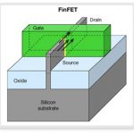
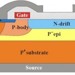
Layouts have also become a factor of smaller geometries, due to effects, such as leakage that affect nearby components. In previous generations of CMOS technologies, all of the transistors had an identical industry standard, a MOSFET (Metal-Oxide Semiconductor Field-Effect Transistor). It is a four terminal device, with the fourth terminal (body or substrate) connected to the source terminal. The layout of the chip design caused little variation, because the simplicity of the MOSFET geometry. Now with new types of geometries for smaller transistors (e.g. FinFet), the layout designs around the transistor may not be as identical as before. Different patterns from the layouts have to be taken into consideration in simulations.
As we make the transition from planar transistors to FinFETs, a new BSIM (Berkeley Short-channel IGFET Model) model is needed in order to properly run the simulations required to ensure a proper functioning circuit. BSIM models are equation based models that are developed at UC Berkeley and supported by CMC (Compact Model Coalition). In order to run the simulations, these models are imported into your design in SPICE. In addition, the transition from planar transistors to FinFETs means more simulation computations. Ravi Subramanian, GM for the analog/mixed-signal group at Mentor Graphics, illustrates that “complexity is measured by the number and type of equation in these models. Going from planar to FinFET, the modeling complexity has increased by over 100X in terms of the raw number of computations required per transistor. That means that for every transistor, you need to do 100X more computations.” [1] The FinFET is one of the factors that adds to the complexity of the simulations. With the channel between source and drain shortened, leakage and Drain-Induced Barrier Lowering (DIBL), a change in threshold voltage and output conductance due to drain voltage, are some of the known negative effects of sub 50nm transistors. The FinFET is a 3D device with the gate wrapped around the channel, which mitigates DIBL and leakage. With the increase electron control, more charge can flow through the inversion region of the channel as the gate switches. The charge variation of the FinFET makes modeling more difficult, because of the changes in the depletion region of the IV curve. With traditional MOSFET devices, variation in the IV curve are most significant to simulations. Now VLSI designers need to take into account the charge variation of the smaller transistor as well as the IV characteristics. [1].
Moreover, the 3D layout has a rather negative impact on the thermal dissipation of the transistor, due to the wire density and overall density of the transistor. The increased heat due to poor dissipation leads to faster degradation and less reliability. Degradation in newer chips can be seen in layout interconnects where their increasing lengths and slim thicknesses and depths, high current density and higher operating temperatures occur. Changes such as replacing aluminum with copper have been made to lessen these effects but electromigration is still a problem as everything is moving to newer and more advanced nodes. When a circuit is active and electrons flow, the electrons can cause damage due to the heat and pressure that they generate within the metal. With the ever increasing push to smaller nodes, this becomes much more important and requires analyzing, where in the past it was only required to analyze sensitive analog blocks and high power blocks used in automotive. [1]
Hot carrier injection (HCI) and bias temperature instability (BTI) also play a part in the degradation of devices. Hot carrier injection occurs when enough kinetic energy injects particles into parts of a circuit that they shouldn’t be in such as the gate dielectric. The displacement of these particles cause “threshold voltage changes and trans conductance degradation in the device” [1]. Bias temperature instability occurs between the silicon dioxide layer and the substrate which causes the absolute threshold voltage to increase which in turn leads to degradation within the device. Hot carrier injection and bias temperature instability are both things that now must be taken into consideration in the libraries. [1]
Process variation increases as the new devices decrease in size. The main contributors to process variation are oxide thickness and mask alignment. Oxide thickness is the insulating pad between the gate and the dopants. To improve performance or size, the oxide thickness is reduced, which would lead to leakage. Moreover, the device is very sensitive to the slightest change in sub-20 nm transistors. Randomness of the variation adds more difficulty to the process, as all devices are no longer equally affected.
In past design procedures, VLSI designers’ solution to variability was to add margins. Due to “the sensitivity to varying parameters”, an even further amount of margins must be added. [1] According to Yoann Courant, R&D Director in the Process Variability Group (PVG) of Silvaco, ‘Monte Carlo is the traditional approach for variation analysis, but it is becoming too costly as thousands of runs are needed in order to statistically converge to an acceptable precision.” [1] He suggests that advanced Monte Carlo techniques are needed to speedup to simulation runs. Monte Carlo is a computational algorithm that obtains numerical results through repetition of random sampling. Recently, Subramanian has noticed a movement to use statistical analysis reasonably. He states, “We are at the early days of this. People are looking at, and starting to use an approach called ‘The Design of Experiments’.” [1] Additionally, people are considering how many simulations are required to attain a good confidence interval for a given situation. If a VLSI designer has a set of measurements, an equal number of experiments relative to the amount of measurements is necessary. In turn, the experiments are used to attain a certain degree of confidence for the initial measurements. [1]
As circuit designers progress to ever smaller processes, margins for error will keep growing tighter and simulations will continue increase in complexity. However, advancements in parallel calculations within newer chips will keep performance increasing without shrinking the manufacturing processes, which adds further complexity to simulations. With the increase in complexity, the right level of model abstraction is the main challenge. Another challenge is to have the proper methodology that enables designers to move in and out between different levels of abstractions for different blocks. A solution to these challenges is SystemVerilog. Verilog is no longer an active standard and with a migration towards SystemVerilog, new features and enhancements to strengthen mixed-signal design and verification are undertaken. SystemVerilog has a higher level of abstraction with specific design intent, meaning VLSI designers have more control over the logic of the design. Additionally, the higher abstraction level allows the VLSI designer to switch between different design levels. VHDL and Verilog users will still recognize certain constructs within SystemVerilog, leading to a smooth transition. For Verilog, existing code will not need any modification, due to SystemVerilog being a superset of Verilog.
By Mike Malory and George Humphrey II
References
[1]”Transistor-Level Verification Returns.” Semiconductor Engineering. Brian Bailey, 13 Jan. 2016. Web. 18 Feb. 2016.
[2]Daniel Payne. (2011). Transistor-Level Electrical Rule Checking [Online]. Available FTP: www.semiwiki.com Directory: /forum/content/ File: 511-transistor-level-electrical-rule-checking.html
[3]IEEE Standard for System and Software Verification and Validation – Redline,” in IEEE Std 1012-2012 (Revision of IEEE Std 1012-2004) – Redline , vol., no., pp.1-223, May 25 2012
Book Review Mobile Unleashed The History of ARM
After having taken a closer look at x86 processor with “Inside The Machine” I came across “Mobile Unleashed“, a book about the history of a non-Silicon Valley company and technology for a change that has significantly shaped the world of computing as we know it today: ARM.
Written by Daniel Nenni and Don Dingee the book tells the story of the ARM microprocessor that powers pretty much everything these days that has a CPU inside except your PC at home and data centers which are (still) mostly dominated by the Intel x86 architecture.
Before reading the book I was vaguely aware that the ARM processor was initially designed by a company called Acorn in the UK as a processor for their BBC Micro successors, the Acorn Archimedes line of computers. That was back in the 1980s and the Archimedes was in direct competition with the Amiga, the Atari and the PC. But apart from that I knew little what happened between then and ARM having become the dominant embedded CPU architecture today that is not only used in smartphones but in pretty much everything else ‘non-PC’.
The authors do a wonderful job of filling my gaps and telling the story of Acorn and ARM at the beginning, how Apple became involved as ARM’s first customer and share owner when they needed a powerful but power efficient and embeddable processor for their Newton PDA and how the ARM architecture spread quickly from then on. They then go on to tell the story of how, unlike Intel who always wanted to be in control themselves about their processor and its production, ARM’s philosophy was different from the start. Their approach was and is to license their design and instruction set and let other companies build their own hardware around it or even design their own processor based on the ARM instruction set to adapt it to their needs and to build their own hardware around it.
In the second half of the book, the authors take a look at three major companies who are using ARM technology in the past and today: Apple with its A7, A8, etc. smartphone and tablet processors, Qualcomm with their platforms for wireless and Samsung with their Exynos chips for their Galaxy branded smartphone flagships. Apart from a great history lesson a major takeaway for me is that while most companies take the processor as designed by ARM, the companies mentioned above go one step further and design their own processor based on the ARM instruction set. Qualcomm is an interesting company in that regard as some of their chips use original ARM processor designs while others use their self designed ARM processor cores, something that would be impossible to do with Intel.
Overall, the book does not only cover the evolution of ARM from the beginning of the 1980s to today but also the history of Samsung, Apple and Qualcomm when it comes to their use of ARM. For Samsung and especially for Qualcomm, the book goes a step further and also contains a short general history of the company. For me it was especially interesting to learn about how Qualcomm came up with their 2G CDMA solution at the end of the 1980’s and positioned it as an alternative to D-AMPS and GSM. What a difference compared to the process in which nation states and state owned telephone monopolies in Europe agreed to come up with a single digital mobile communication system in the 1980’s. A miracle GSM succeeded in the massive way it did despite so many people, companies and nations who wanted to have a say.
In summary, if you want to learn more about the British computing industry in the 1980’s, about ARM, some history about Apple, Samsung and Qualcomm and get a perspective on the mobile industry with a ‘silicon angle’, then “Mobile Unleashed” is the book to read!
Webinar alert – Taking UVM to the FPGA bank
UVM has become a preferred environment for functional verification. Fundamentally, it is a host based software simulation. Is there a way to capture the benefits of UVM with hardware acceleration on an FPGA-based prototyping system? In an upcoming webinar, Doulos CTO John Aynsley answers this with a resounding yes. Continue reading “Webinar alert – Taking UVM to the FPGA bank”
Webinar alert – Smart homes demanding low power Wi-Fi
There are two camps of thinking on the IoT: those who believe Bluetooth and Wi-Fi rule the edge, and those who support any of dozens of other wireless networking specifications for their various technical advantages. The ubiquity of Wi-Fi in homes helps devices connect in a few clicks – so why don’t more IoT designers use it? Continue reading “Webinar alert – Smart homes demanding low power Wi-Fi”
3D TCAD Simulation of Silicon Power Devices
Process and device engineers are some of the unsung heroes in our semiconductor industry that have the daunting task of figuring out how to actually create a new process node that will fit some specific, market niche with sufficient yield to make their companies profitable and stand out from the competition. One such market segment is silicon power devices where the transistors are used to charge or switch a battery, control an electric motor, make a power supply, lighting control, automotive controls, or drive a discrete power device. In the early days the engineers would design a process experiment, fabricate, then take measurements to analyze how effective their ideas were, iterating until satisfied.
Today we cannot tolerate such slow iteration cycles, so instead we turn to specialized EDA software called 3D TCAD where the process and devices can be modeled and simulated to predict their electrical performance prior to actually fabrication. Silvaco is hosting a webinar on April 14th to show us how a 3D TCAD simulation can be done for silicon power devices.
LDMOS device cross-section
The webinar looks at how to apply both 2D and 3D cell design for vertical LOCOS (LOCal Oxidation of Silicon) power devices. Another application area for 3D TCAD is the 3D current filaments simulation for multi-cell IGBT (Isolated Gate Bipolar Transistors). On the software side the Silvaco tool called Victory Device will be shown:
- Architecture of the software
- 3D rapid prototyping to detailed physical simulation
- Meshing approach
- Solvers
3D electric field distribution. Field is maximum at the corner of the trench.
Who should attend a webinar like this on 3D TCAD? If you’re a power device designer, power device process development engineer, production engineer, power device researcher, or a materials researcher then this webinar is going to be relevant. Using a TCAD tool like Victory Device shows you the electrical and thermal behavior of: Power MOS, LDMOS, SOI, thyristors and IGBTs. You can even model and simulate wide bandgap materials like SiC and GaN. The devices that you model can be embedded with a circuit then simulated with a SPICE circuit simulator to look at timing, current and power performance.
Using TCAD software enables you to do electrical, thermal and optical characterization of semiconductor devices, pus optimize the performance by making rapid iterations. This TCAD methodology will actually reduce the total process development time. You can even explore novel device technologies for use in next-generation devices.
Even though this webinar is focusing on power device users, with a TCAD tool like Victory Device you and model and optimize CMOS devices like FinFET and FDSOI. Here’s an example 3D FinFET simulated with a 3D fully unstructured tetrahedral mesh:
Even compound semiconductors can be modeled and optimized: SiGE, GaAs, AlGaAs, InP, SiC, GaN, AlGaN, InGaN. Optoelectronic response for devices like solar cells and CMOS image sensors can also be simulated. Finally, you can even model the effects of radiation like: single event upset (SEU), single event burnout (SEB), total dose and dose rate.
Webinar
This webinar is scheduled for April 14th at 10AM PDT, so sign-up today online.
Related Blogs
Mobile Unleashed…Reviewed
I finished reading Don Dingee and Dan Nenni’s book, Mobile Unleashed, the Origin and Evolution of ARM Processors in Our Devices. I guess by way of disclosure I should say that Don and Dan both blogged with me here on SemiWiki for several years before I joined Cadence, and Dan’s last book Fabless was co-authored with me (SemiWiki members can download it free). So I don’t claim complete objectivity.
Let me start by pointing out that this is a book for professionals in the mobile and semiconductor industries. This is both its strength and its weakness. You will learn a lot of things you didn’t know, even if you have been in the industry for decades. On the other hand, this is not the book to give to your mother to give her more of an idea about what you do all day. But as it says in the foreword:
We have waited over two decades for someone to tell this story.
Since the foreword was written by Sir Robin Saxby, the original CEO of ARM, this is high praise indeed.
You probably know the big picture story of ARM. Back in the day before the IBM PC, when there were dozens of different computer architectures, a company called Acorn won the contract to build the computer around which the British Broadcasting Corporation (BBC) created a series of educational television programs about computers and programming. Acorn struggled to repeat that success and took the decision that none of the commercially available microprocessors met their needs and so they would build their own microprocessor. In retrospect this was a great idea, but in some ways at the time it must have looked like something somewhere between insane and the ultimate in NIH (not-invented-here). The book covers this in more detail than I have seen before.
The processor was not a success and Acorn continued to struggle and was acquired by Olivetti, which soon was only interested in IBM PC-compatible products for the business market. The big stroke of luck came when Apple decided to build the Newton. The original ARM® processors were not designed specifically to be low power, nobody cared back then. But with its very simple architecture, it delivered the highest performance per watt of any processor available. Since the Newton needed reasonable power to do handwriting recognition, but also had to run on batteries, this was a really important measure and they selected ARM. But they insisted Acorn/Olivetti spin it out as a standalone company and so ARM was created (the A stood for Acorn originally, before it changed to Advanced).
The next big development was between TI (Wally Rhines, as it happened, before he became CEO of Mentor) and Nokia and ARM. One disadvantage of a 32-bit RISC architecture was that the code density was not good, since every instruction took 32 bits. On the plane on the way home from the meeting at Nokia the idea of what became Thumb was already well along: a mode in which the ARM would use 16-bit instructions, expand them to 32-bit and feed them to the original decoder. Code density would be good, and they wouldn’t need to do a complete redesign (this was before synthesizable cores). Thus, the ARM7TDMI was born, with the project lead being Simon Segars, who is ARM’s CEO today.
See my interview with Simon Segars, The Design that Made ARM
Nokia grew to about a third of the entire mobile industry as first car phones and then mobile phones in general took off and became ubiquitous. ARM found itself sitting on a rocket ship as two things happened. Microprocessors became a small enough part of a chip that early SoCs could be designed with an embedded microprocessor and other circuitry. Suddenly every semiconductor manufacturer needed a microprocessor if they didn’t have their own in-house one already, and there weren’t very many choices available for license. Plus, with mobile taking off, everyone wanted to participate. So many (eventually most) semiconductor companies licensed the ARM7TDMI.
That takes the history of ARM to its second phase. The early days of ARM history are gradual: the architecture, the first ARM, the spinout, the ARM7, Thumb, mobile. But the second phase began in just an hour. Steve Jobs walked onto the stage of YBCA and said he would be announcing three new products:The first one is a widescreen iPod with touch controls. The second is a revolutionary mobile phone. And the third is a breakthrough Internet communications device.
Of course, we all now know that all three products were one, the first iPhone. And the world changed.
It wasn’t even obvious at the time how much it was changing. The CEOs of both Microsoft and Nokia dismissed it as just a handset. Both companies would effectively be driven from the mobile market by iPhone and its Android imitators.
The second half of Mobile Unleashed is the smartphone era. It doesn’t cover everything or it would be unreadable. It focuses on a few companies: Apple, Samsung, and Qualcomm. These are the right companies to focus on since they make all the money. The rest of the handset market, in aggregate, loses money. The story of each company is told in some detail: how they entered mobile and what they have done to keep competitive as the computational power expected of a smartphone has exploded but the power budget has remained roughly constant.
The book wraps up with a look into the future, in particular the market for wearables and Internet of Things (IoT), and the briefest mention of servers. But as the last chapter before the epilogue ends:The next chip that changes the world may come from any number of sources, but there is a good chance it will run on ARM technology.
There is a book called Certainly More Than You Want to Know About the Fishes of the Pacific Coast. If you don’t have a background in the semiconductor industry then this book will certainly tell you more than you want to know about ARM processors. But if you do have a background in the semiconductor industry then this is a book well worth reading. No matter how much you know about ARM and Apple and Qualcomm, Don knows more, and you will learn a lot.
This is actually cross-posted from Breakfast Bytes over at Cadence. If you wondered why I vanished from Semiwiki and haven’t found out yet, then go there and take a look. I put out a blog every day, sometimes about something Cadencey but most of the time not (the last couple of days have been CDNLive Silicon Valley so you can expect some coverage of the parts I attended, although with 12 parallel tracks that is a fraction of what was available).
Click here and check out my new home. There are already over 100 blogs up. There is a box towards the top right where you can subscribe and get an email whenever I post, which, like my blogs on Semiwiki. is normally 5am Pacific, unless it is tied to a Cadence press release (they don’t cross the wire until 7.45am). Get something interesting to read with your morning coffee.
Breakfast Bytes, fresh every morning.

