Krishna has over 30 years of expertise in the semiconductor industry, holding senior roles at Rambus, AMD and Broadcom. As a serial entrepreneur, he co-founded SCI Semi Ltd and previously established DataTrails and Secure Thingz.
Tell us a bit about your career background. What are you most proud of?
Over the course of my 30 year career in the global semiconductor industry, I have been fortunate to work across a broad range of roles. My first job was as a digital circuit designer, then I gradually transitioned into marketing, business development and corporate management positions with major semiconductor players such as Rambus, AMD and Broadcom. I am proud of the fact that I have been able to draw on my extensive experience, network and industry knowledge to help establish cutting-edge companies, including SCI Semiconductor, DataTrails and Secure Thingz.
Why did you decide to join Agile Analog?
I was invited to advise Agile Analog on its product roadmap and Go-To-Market strategy. After spending time with the team and technology I was highly impressed by the capabilities of the Composa tool and the quality of IP generated through the automation platform. The strength of customer engagements and recent project deliveries further validated the company’s great potential. I am passionate about working with entrepreneurial teams, and Agile Analog represents a unique opportunity to leverage my experience in engineering, GTM and P&L management to help drive revenue growth and scale the business.
What key problem is Agile Analog solving?
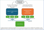
The shortage of skilled analog engineers in the semiconductor industry is a significant problem. Composa addresses this gap by enabling the rapid automation, design and redesign of mixed-signal IP blocks – whether adapting to changing specifications or migrating across process nodes. This is a solution the industry has long been waiting for – helping to radically reduce the complexity, time and costs associated with traditional analog design.
What are your main focus areas and challenges over the next six months?
Agile Analog offers an expanding portfolio of IP across data conversion, power management, IC monitoring, security and always-on IP. Over the next six months, the focus will be on building strategic industry partnerships and delivering integrated subsystem level IP solutions. There is clear market demand for our customizable, process agnostic products. As a lean organization, our key challenge is prioritizing our roadmap and aligning our efforts with the industry verticals that present the greatest potential for scalable growth.
What markets and applications are the company’s strongest?
Agile Analog has secured business wins across a wide range of verticals and applications, including consumer, enterprise data centers, security, space and industrial sectors. Analog security IP and anti-tamper IP are a big focus for us at the moment. Security has become a critical consideration for every SoC being developed today and our security IP products are ideally suited to address this.
What new product developments are your team working on?
The Agile Analog team is working to expand our portfolio of security IP and anti-tamper IP beyond our existing voltage glitch detector and clock attack monitor IPs, in order to be able to detect a wider range of physical attacks. Another important area for us is developing our range of data conversion solutions to include higher resolution and higher sample rate solutions. We are seeing great interest in our existing products across process nodes and we are just about to start working on bringing our ADC to the latest TSMC node for one of our strategic customers.
What is the long-term vision for Agile Analog?
Agile Analog’s unique technology, Composa, is our key differentiator from other analog IP companies. With the power of automation, we can quickly deliver IP tailored to precise specifications and process nodes. Our vision is to become the leading provider of high-value analog subsystem IP and licensable automation tools that enable accelerated IP development.
Which industry events are Agile Analog attending this year and why?
2025 has already been a busy year for Agile Analog, with the team taking part in many of the major foundry events held by Intel, TSMC and Samsung. In late June we will be at DAC and then in the second half of the year we will be going to the GlobalFoundries events, as well as more TSMC events. It’s pretty full-on!
Also Read:
2025 Outlook with Christelle Faucon of Agile Analog
Overcoming obstacles with mixed-signal and analog design integration