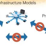
RVN! 26 Banner revised (800 x 100 px) (600 x 100 px)

The Driver in the Driverless Car

The Driver in the Driverless Car
by Vivek Wadhwa on 04-09-2017 at 8:00 am

What is the likelihood that the people building Uber’s self-driving technologies did not know that their software was highly imperfect and could endanger lives if the cars were let loose on public streets? Or that employees of Theranos did not know that their equipment would produce inaccurate diagnostics?

San Francisco has had some close calls with the self-driving Uber vehicles, though no damage has resulted. But Theranos did negatively affect the lives of tens of thousands of people. Should the Uber and Theranos employees who remained silent share the burden of guilt? I would argue that they should and that anyone who stays silent when they see wrongdoing is complicit in the injustice.

I know that I am taking a strong stand, and that employees have to worry about their livelihoods and families; that they may believe that they don’t have the power to change anything, it being the job of the CEO to make the difficult decisions. And, yes, I know that these examples are extreme.

But as technology advances, its reach and power grow exponentially. Even its creators don’t understand the use cases and long-term impacts of their products. What makes it worse is that CEOs are responsible to shareholders and obsess over making money, and workers are responsible to their employers. Who is watching out for humanity itself?

As I explain in my forthcoming book, The Driver in the Driverless Car, technologies are advancing exponentially. Our smartphones are already more powerful than the supercomputers of yesteryear. By 2023, at computers’ present rate of advancement, the iPhone 11 or 12’s ability to process and store information will exceed that of the human brain (I am not kidding).

This growth applies not just to smartphones and PCs but to every technology, including sensors, networks, artificial intelligence, synthetic biology, and robotics.

We could, within two or three decades, be in an era of abundance, in which we live long and healthy lives, have unlimited clean energy and education, and have our most basic wants and needs met. Because of these advances it is becoming possible to solve the grand challenges of humanity: hunger, disease, education, and energy.

Yet these advances have a potential dark side. As easily as we can edit genes, we can create killer viruses and alter the human germ line. Self-driving cars can bring mobility to the blind, but they can also take lives. And we could lose whatever is left of our privacy as connected devices take over our homes.

This is why we all need to learn to see the big picture and to understand our responsibilities. We need to be aware of our technologies’ potential for misuse and to build safeguards. We need to speak up when we see wrongdoing and to document the risks.

In my free LinkedIn Learning course, I share the key lessons that product managers, developers, and designers must pay attention to, and I explore their roles and responsibilities—for instance, what responsibility Facebook employees have for use of their technologies to spread fake news and disrupt elections.

In The Driver in the Driverless Car, I go much further and discuss why this is the most amazing—and scary—period in human history. I illustrate a broad range of technologies and discuss their value to society and mankind. I ask you to consider whether they have the potential to benefit everyone equally, the balance between their risks and potential rewards, and whether they more strongly promote autonomy or dependence. It is fairness and equality that are at the heart of these questions. Many technologies are going to disrupt present-day industries, causing our lives to change for the better and for the worse. Just one consequence of this will be the loss of tens of millions of jobs. If we manage that loss equitably and ease the transition and pain for the people who are most affected and least prepared, we can get to the utopian world of the TV series Star Trek. The alternative is the dystopia of Hollywood’s Mad Max.

It is the choices we make that will determine the outcome—beginning with the choices we make at work.

You can also follow on Twitter: @wadhwa and visit my website: www.wadhwa.com


The Fate of Autonomous

The Fate of Autonomous
by Roger C. Lanctot on 04-09-2017 at 7:00 am

The latest installment in the “Fast and Furious” franchise will debut bringing the concept of remote control of cars into the mainstream. Suffice it to say that remote control plays a major role in the script.

This will only be the latest chapter of a long-running effort to demonize autonomous vehicle technology in mass media – preceded just this week by an Uber self-driving car being upended by a human driven vehicle in Arizona leading to the temporary suspension of Uber’s testing program.

– “Uber Halts Self-Driving Car Tests After Arizona Crash”


“Fast and Furious” is all about humans driving cars, though the movies glamorize human driving for illicit purposes. So I guess the virtues of both human and machine driving are equally disparaged in the films.

About 10 years ago, a now-retired BMW executive told me that car makers arguably bear a responsibility to seize control of their vehicles remotely if 1) they have the technology capable of doing so and 2) the vehicle is being used with ill intent, the driver is incapacitated or the vehicle malfunctioning. The terror attack in London last week highlighted just such a scenario.

Khalid Masood deliberately drove his rented SUV into pedestrians on London Bridge before crashing the car and proceeding to attempt to enter Parliament before being killed by responding officers. The entire incident consumed 82 seconds and took five lives, according to press reports.

Khalid Masood’s rented SUV post-crash. SOURCE: BBC


There are a number of important implications here for safety systems and autonomous vehicle operation. Police officers in the UK and elsewhere in the world note that some of the latest safety systems such as collision avoidance actually prevent police officers from using so-called “pit” maneuvers to disable fleeing felons. Noting Masood’s path down the sidewalk on London Bridge, one can envision a future world where driving onto the sidewalk was rendered impossible by safety systems or autonomous driving technology.

Straying onto the sidewalk might also be prevented or corrected remotely in the future. From human-piloted rovers on the moon mankind has proceeded to remotely-piloted rovers on Mars. The same technology was demonstrated by Nissan at the CES show in Las Vegas in January and by Ericsson at Mobile World Congress in Barcelona.

Described by Nissan as “teleoperation,” executives from Nissan’s Sunnyvale Tech Center demonstrated the company’s Seamless Autonomous Mobility platform – remotely operating a car using LTE wireless connectivity. The application demonstrated by Nissan was remotely taking control of a car that is experiencing an unexpected and perhaps dangerous event such as an incapacitated driver.

– Nissan Uses Rover Tech to Remotely Oversee Autonomous Car

The Nissan demonstration was compelling, but it highlighted the limitations of remote human operation of an autonomous vehicle. Taking control remotely can be as terrifying as re-taking control locally in the car. More often than not, events are occurring too rapidly for a human to respond – as in the case of the over-turned Uber vehicle in Arizona.

The point is that remote operation used in conjunction with autonomous driving technology and advanced safety systems can prevent crashes and criminal activity. Hyundai recently had the opportunity to show off its BlueLink immobilization application to prevent a vehicle theft in Atlanta.

– “Atlanta Police Make Quick Arrest Thanks to Technology in Grandmother’s Stolen Car”

Autonomous technology and remote control are introducing profound changes in how humans interact with their machines. Nowhere is this profound shift more pronounced than in the Tesla Motors’ Model S’s equipped with Autopilot 2.0.

Owners of the Model S that upgraded from Autopilot 1.0 to 2.0 saw significant changes in the operation of their vehicles – losing access to the function in certain areas (geo-fencing of the feature) and experiencing new speed restrictions. Over time, as the vehicles were able to take advantage of machine learning and further software upgrades some performance has been restored.

At the same time, though, Autopilot in the Model S now requires the operator to periodically put his or her hands on the steering wheel thanks to software updates. Failure to comply with this requirement results in temporary loss of access to the Autopilot mode.

In essence, humans have been teaching cars how to drive for the past 10 years and now cars are returning the favor. In the future, if you cannot obey the rules of the road or at least the rules for operating your particular motor vehicle you may lose the privilege of operating that car at least temporarily.

The horrific incident that occurred in London last week might well have been prevented either by appropriately tuned safety systems designed to prevent the car from leaving the roadway or from a vigilant remote monitoring system capable of taking control or immobilizing the errant vehicle. The “Fate of the Furious” may demonstrate the terroristic potential of massive remote vehicle operation, but the reality is that technology is ultimately mankind’s friend if developed and deployed appropriately.

With a little luck and some clever algorithms we humans will come to view the arrival of autonomous driving as the onset of a helping hand rather than robots gone wild. In the end we’re less concerned with criminal activity and terror and more interested in the ability of autonomy to make every day driving more pleasing.

Roger C. Lanctot is Director, Automotive Connected Mobility in the Global Automotive Practice at Strategy Analytics. More details about Strategy Analytics can be found here:

https://www.strategyanalytics.com/access-services/automotive#.VuGdXfkrKUk


14nm 16nm 10nm and 7nm – What we know now

14nm 16nm 10nm and 7nm – What we know now
by Scotten Jones on 04-07-2017 at 7:00 am

Last week Intel held a manufacturing day where they revealed a lot of information about their 10nm process for the first time and information on competitor processes continues to slowly come out as well. I thought it would be useful to summarize what we know now, especially since some of what Intel announced was different than what I previously forecast.
Continue reading “14nm 16nm 10nm and 7nm – What we know now”


The Rise of Transaction-Based Emulation

The Rise of Transaction-Based Emulation
by Bernard Murphy on 04-06-2017 at 12:00 pm

One serious challenge to the early promise of accelerating verification through emulation was that, while in theory the emulator could run very fast, options for driving and responding to that fast model were less than ideal. You could use in-circuit emulation (ICE), connecting the emulation to real hardware and allowing you to run fast (with a little help in synchronizing rates between the emulation and the external hardware). But these setups took time, often considerable time, and had poor reliability; at least one connection would go bad every few hours and could take hours to track down.


Alternatively, you could connect to a (software-based) simulator testbench, running on a PC, but that dragged overall performance down to little better than running the whole testbench + DUT (device under test) simulation on the PC. For non-experts in the domain, testbenches mostly run on a PC rather than the emulator, because emulators are designed to deal with synthesizable models, while most testbenches contain logic too complex to be synthesizable. Also emulators are expensive, so even if a testbench can be made synthesizable, there’s a tradeoff between cost and speed.

ICE for all its problems was the only usable option but was limited by cost and value in cases where setup might take nearly as much time as getting first silicon samples. More recently, ICE has improved dramatically in usability and reliability and remains popular for live in-circuit testing. Approaches to software-based testing have also improved dramatically and are also popular where virtualized testing is considered a benefit, and that’s the subject of this blog. (I should note in passing that there are strong and differing views among emulation experts on the relative merits of virtual and ICE-based approaches. I’ll leave that debate to the protagonists.)

There are two primary reasons that simulation-based testbenches are slow – low level (down to signal-level, cycle-accurate) modeling in the testbench and massive amounts of signal-level communication between the testbench and the DUT. Back in the dawn of simulation time, the first problem wasn’t a big deal. Most of the simulation activity was in the DUT and the testbench accounted for a small overhead. But emulation (in principle) reduces DUT time by several orders of magnitude, so time spent in the testbench (and PLI interfaces) becomes dominant. Overall, you get some speed-up but it falls far short of those orders of magnitude you expected.

This problem becomes much worse when you think of the testbenches we build today. These are much more complex thanks to high levels of behavioral modeling and assertion/coverage properties. Now it is common to expect 50-90% of activity in the testbench (that’s why debugging testbenches has become so important); as a result traditional approaches to co-simulation with an emulator show hardly any improvement over pure simulation speeds.
One way to fix this problem is to move up the level of abstraction for the testbench to C/C++. This is a popular trend, especially in software-driven/system level testing where translating tests to SV/UVM may become challenging and arguably redundant. (SV/UVM still plays a role as a bridge to emulation.) Now testbench overhead can drop down to a very small percentage, delivering much more of that promised emulation speedup to total verification performance.

But you still must deal with all that signal communication between testbench and emulator. Now the botteleneck is defined by thousands of signals, each demanding synchronized handling of cycle-accurate state changes. That signal interface complexity also must be abstracted to get maximum return from the testbench/emulator linkage. That’s where the second important innovation comes in – a transaction-based interface. Instead of communicating signal changes, you communicate multi-cycle transactions; this alone could allow for some level of speed-up.

But what really makes the transaction-based interface fly is a clever way to implement communication through the Standard Co-Emulation Modeling Interface (SCE-MI). SCE-MI is an Accellera-defined standard based on the Direct Programming Interface (DPI) extension to the SV standard. This defines a mechanism to communicate directly and portably (without PLI) between an abstracted testbench and an emulator.

The clever part is splitting communication into two functions, one running on the emulator and the other on the PC. On the emulator, you have a synthesizable component assembling and disassembling transactions. On one side, it’s communicating with all those signals from the DUT and can run at emulator speed because it’s synthesized into emulator function primitives. On the other side, it communicates transactions to a proxy function running on the PC.

Now you have fast performance on the emulator, fast (because greatly compressed) communication between PC and emulator, and fast performance in the testbench. All of which makes it possible to rise closer to the theoretical performance that the emulator can offer. It took a bunch of work and a couple of standards but the payback is obvious. What’s more, tests you build should be portable across emulation platforms. Pretty impressive. Mentor has a white-paper which gives more details.


Machine Learning Accelerates Library Characterization by 50 Percent!

Machine Learning Accelerates Library Characterization by 50 Percent!
by Daniel Nenni on 04-06-2017 at 7:00 am

Standard cell, memory, and I/O library characterization is a necessary, but time-consuming, resource intensive, and error-prone process. With the added complexity of advanced and low power manufacturing processes, fast and accurate statistical and non-statistical characterization is challenging, creating the need for a new class of tools to address these challenges.

Many elements within standard cells, memory, and I/O follow similar trends under differing conditions, for example: cell families have similar topology but are just sized differently, differing arcs often show similar behaviors, and PVT (process, voltage, temperature) corners show similar trends but are shifted, scaled or skewed.

Because of these similar trends, library characterization can be accelerated with machine learning technologies. Existing data can be mined for trends, and new library models can be built from previously characterized libraries, but as these library models are built, there is also a need to ensure Monte Carlo accurate LVF/AOCV/POCV library models.

Solido, an EDA industry leader in machine learning technologies, has newly launched ML Characterization Suite–an exciting new tool able to meet these increasing characterization demands. Their continuing success with Variation Designer has placed them in a unique position to develop tools to leverage large scale trends in characterization and mine existing data for trends, all while keeping accuracy paramount.

Within Solido ML Characterization Suite are Predictor and Statistical Characterizer products. Predictor works by:

  • Reading in existing characterized libraries,
  • Determining the PVT corner conditions and turning them into variables and values,
  • Building regression models to predict Liberty values at other PVT conditions,
  • Writing out new Liberty files at new PVT corners.


Solido ML Characterization Suite Predictor has been shown by customers in production to reduce library characterization runtimes by 30% to 70% without compromising accuracy. It’s now instantly possible to produce more libraries for additional PVT corners, saving days to weeks in characterization time and saving on SPICE simulator and characterization resources. Predictor is easy to add into any characterization flow, and works with all Liberty data – NLDM, CCS, CCSN, AOCV, LVF, ECSM, etc.

The second component in ML Characterization Suite is Statistical Characterizer. Statistical Characterizer works by:

  • Reading existing libraries without LVF/AOCV/POCV statistical data,
  • Selecting simulations to produce accurate LVF/AOCV/POCV data for all corners and to parallelize simulations efficiently,
  • Adaptively selecting additional simulations where more accuracy is needed,
  • Writing existing libraries with LVF/AOCV/POCV added.


This technique generates statistical library models with Monte Carlo and SPICE accuracy over 1000 times faster than brute force Monte Carlo. Statistical Characterizer also precisely handles non-Gaussian distributions, all while delivering true 3-sigma LVF/AOCV/POCV.

For even greater statistical characterization savings, Statistical Characterizer and Predictor can be used in tandem for fast, accurate statistical characterization. By using Statistical Characterizer only on anchor corners to quickly add Monte Carlo accurate LVF/AOCV/POCV, then running Predictor to create the remaining corners, Statistical Characterizer only needs to be run on half of the PVT conditions.

ML Characterization Suite Predictor and Statistical Characterizer are available immediately. Sign up here for a 15min demo.

About Solido Design Automation
Solido Design Automation Inc. is a leading provider of variation-aware design software for high yield and performance IP and systems-on-a-chip (SOCs). Solido plays an essential role in de-risking the variation impacts associated with the move to advanced and low-power processes, providing design teams improved power, performance, area and yield for memory, standard cell, analog/RF, and custom digital design. Solido’s efficient software solutions address the exponentially increasing analysis required without compromising time-to-market. The privately held company is venture capital funded and has offices in the USA, Canada, Asia and Europe. For further information, visit www.solidodesign.com or call 306-382-4100.


Integrated Photonics Accelerates with Entrance of TSMC and TowerJazz Foundries

Integrated Photonics Accelerates with Entrance of TSMC and TowerJazz Foundries
by Mitch Heins on 04-05-2017 at 12:00 pm


I’m writing this from the Boston airport on my way home from four straight weeks of PIC (photonic integrated circuit) related travel. It’s been a grueling but very rewarding four weeks and the big take away from this month is that there are now many more signs in the market that integrated photonics is reaching a real tipping point.

I started off March by traveling to Brussels, Belgium to attend the PIC International Conference. This was PIC International’s second year and attendance grew from 440 attendees last year to over 550 this year. This was echoed at the Optical Fiber Conference held in Los Angeles which boasted 14,500 attendees and over 663 exhibitors. The conference was packed with talks about how the industry is girding for the explosive data growth expected to be driven by IoT and 5G cellular. Another key indicator of growing momentum was a 30% increase in attendance of conference short courses meant to educate professionals on the technical aspects of photonics.

The real buzz however, came with several noteworthy news items in March. Among them was a press release by Luxtera where they announced they will be offering a high performance silicon photonics platform with TSMC. The new platform will enable system-on-chip integration of optical interconnect with CMOS logic and will be leverage TSMC’s 7nm CMOS technology. The Luxtera platform is targeting next-generation silicon photonics solutions to deliver 100G-per-lane optical interconnects, starting with 100GBase-DR and 400GBase-DR4 transceivers which they anticipate launching in 2018.

This was promptly followed by a press release from TowerJazz where they too announced they will be providing a new Silicon Photonics process targeting the Optical Transceiver Electronics market. The TowerJazz SiPho process will be based on their SiGe BiCMOS process. When you start seeing production foundries like TSMC, TowerJazz and GLOBAL FOUNDRIES (as announced late last year) getting into the market you know the significant volumes are on their way. This is big!

And lastly, of note was an offer was made by IDT to purchase GigPeak for $250M. GigPeak offers optical interfaces for communications, data centers and military and avionic modules. GigPeak had record profits for its fourth quarter and fiscal 2016 with shipments of its 40 Gbps QSFP+ and 100Gbps QSFP28 ICs for active optical cables (AOCs) and optical transceiver modules into data center customers. The company is also currently sampling driver and trans-impedance amplifier (TIA) ICs for 200 Gbit/s short-reach and long-reach PAM4 Ethernet applications.

The second week of my travels was spent on the east coast of the U.S. traveling up and down the I-90 corridor. One of the most interesting observations of that week was the uptake in the number of integrated photonics projects coming from commercial companies versus past activity which was primarily driven by universities and R&D labs. This was echoed by Twan Korthorst, CEO of PhoeniX Software, where he presented a graph at the PIC International Conference showing a shift of new PhoeniX users coming from commercial companies as opposed to academia. On a side note, PhoeniX’s OptoDesigner tool won the EPIC Award at this year’s PIC International show in the design and test category. While good news for PhoeniX, the interesting part for the reader is that more than 6000 engineers cast ballots for this award. That’s a lot of people for a nascent industry. It also explains PhoeniX’s 45% CAGR for PIC tools over the last four years.

The final week of my travels was spent in Boston at the MIT campus where I attended an AIM Photonics sponsored meetings to road map requirements for the integrated photonics ecosystem. In many cases members were excited to see road map items being accelerated forward by industry.

One of the most interesting presentations was given by Microsoft where they presented on their integrated photonics work used in Time-of-Flight (ToF) cameras and sensors. These cameras give full 3D imaging information for applications such as facial recognition security features. ToF sensors are already in the iPhone 7 and could be applied to future laptops, phones, TVs and gaming consoles. Cameras with 3D depth capabilities can be applied to a wide variety of applications such as gaming, in-air gesturing and augmented reality.

Microsoft, Apple, Intel and Google are all working to bring this ToF technology to bear. Now that would represent some real volume.

This is just the beginning as engineers are barely scratching the surface of what can be done with integrated photonics. From long haul telecommunications, RF and microwave applications, WIFI networks and data center switches, to high volume applications in automotive, mobile devices, industrial sensing and medical and bio-sensing arenas, it’s time to start placing your bets. Hang on to your hats. It’s going to be a wild ride for the next decade!

See also:
Luxtera and TSMC Collaborate on NexGen Silicon Photonics
TowerJazz Announces Silicon Photonics Offering
IDT Makes Offer on GigPeak
PhoeniX Software Selected for PIC Design & Test Award


When Will we Replace the 3.5 mm Jack in Modern Phones?

When Will we Replace the 3.5 mm Jack in Modern Phones?
by Eric Esteve on 04-05-2017 at 7:00 am

You have certainly experienced that modern mobile phones are used for more than phone calls and do not have room for multiple connectors. A new approach for audio connectivity is needed, allowing product designers to retire the 3.5mm jack. Considering the USB audio protocol to replace the analog audio solutions, typically using a 3.5mm phone jack, seems to be the obvious solution, but the legacy USB audio cannot replace the 3.5mm phone jack in mobile phones and other portable, battery powered products, as it would drain the battery too quickly.

The modern solution was announced on September 27, 2016 by the USB-IF, it’s the USB Audio Design Class (ADC) 3.0…

ADC 3.0 is expected to be the new standard for phones using the USB Type-C[SUP]TM[/SUP] connector, because, unlike legacy USB audio protocols, ADC 3.0 implementations is enabling significant system power savings, which are critical to low-power mobile applications.

Before describing how ADC 3.0 implementation enable power savings, let’s take a look at the power profiles for mobile phone with analog headset. For analog audio solutions, the communication between the source and the user is burst based, allowing functional blocks to enter lower power modes between bursts of activity. It’s a pretty efficient solution in term of power consumption, but it’s using the 3.5mm phone jack and the goal is to remove it.

Unlike analog headsets, USB audio headsets use isochronous transfers. Isochronous transfers provide the guaranteed bandwidth which is required for audio streams, but at the cost of a higher power consumption. To strongly reduce this power consumption, the USB ADC 3.0 is smartly using the new power state Link Power Management (LPM L1) for High Speed USB.

Isochronous transfers for legacy USB audio occurs every 1ms for Full Speed USB. The bus is idle between transfers, but cannot enter Suspend L2. The combination of High Speed USB bursting and LPM L1 Suspend offers significant power savings opportunities. The next figure shows the power saving events of the new audio specification as a function of time.

Integrating the USB 2.0 LPM L1 specifications seems to be a good option to reduce the power consumption in such a way that USB ADC 3.0 could replace analog audio solution, and the USB Type-C connector replace the 3.5 mm jack. But a proof of concept was required to allow the ADC 3.0 specification to progress. Synopsys has demonstrated the successful proof of concept using Synopsys DesignWare® USB IP.
I suggest you to read this articlewritten by Morten Christiansen, Technical Marketing Manager, Synopsys, and I recommend you spend some time on the Figure 4: “Proof of concept for LPM L1 power save”. You will go deep inside the packet based USB protocol and understand how LPM L1 really works. In this system used for the proof of concept, the LPM L1 Suspend residency is 87.8% (3.513ms of a 4ms service interval).

The author reminds that PHY power consumption is important to consider alone, as it is typically much higher than controller power consumption. LPM L1 power is typically less than 1% of active or idle power and using LPM L1 can result in PHY power savings of 86%. And the conclusion is that USB Audio Device Class 3.0 USB headset solutions that are power-competitive with legacy analog headset solutions.

To implement ADC 3.0 in low-power products like phones, tablets or laptops, designers will need an ADC 3.0 compliant host controller with Hardware Controlled Link Power Management capability. The ADC 3.0 compliant device controller implementation will require some important changes and designs supporting ADC 3.0 require LPM L1 capable PHYs. Synopsys is claiming that lead customers are already designing ADC 3.0 compliant headsets using industry leading LPM-capable USB IP.
As an end user, we should have the opportunity to buy smartphones equipped with a single connector in the near future. USB Type-C specification allowing to support Power Delivery, Authentication, Audio (ADC 3.0) is expected to see large adoption as 2 billion+ units are forecasted by IHS to ship in 2019, or 40% of total units.

The article from Synopsys about USB Type-C ADC 3.0:
https://www.synopsys.com/designware-ip/newsletters/technical-bulletin/usb-audio-dwtb-q117.html
By Eric Esteve from IPnest


When Once is Not Enough, But Unlimited is Too Much

When Once is Not Enough, But Unlimited is Too Much
by Tom Simon on 04-04-2017 at 12:00 pm

When people think about non volatile memory, the first thing that usually comes to mind is NAND flash like that used in SSD’s or in microcontrollers to hold on-board code. Of course, there is also EEPROM and other types of NVM as well that can be used to hold data and code for the multitude of connected devices that are so common now. For many SOC designs NAND flash or EEPROM might be the go-to technology for re-writeable persistent storage. However, there are some down sides to this technology, and there is an attractive alternative worth considering. So, what might make SOC designers think twice about going with NAND flash?

I learned more about the specifics of this while I was at the TSMC Technology Symposium on March 15[SUP]th[/SUP]. I had the opportunity to have lunch with Ken Wagner, Sr. VP of Engineering, and Andrew Faulkner, Sr. Director of Marketing, at Sidense, provider of one time programmable (OTP) IP for integration into SOC’s.

The top drawback for considering adding NAND flash or many other NVM’s is that they require additional mask layers or special processes. These requirements cost more money, introduce risk and can limit options for fabrication. In many applications security and durability are essential. Technologies that use charge storage can be perturbed and suffer data loss. They are also vulnerable to thermal degradation. IoT devices and mobile devices can be subjected to intense environmental conditions. Another application where heat is a significant factor is in the automotive arena. Floating charge devices can be probed externally to reveal their contents. Side channel attacks can also sometimes decipher the contents of flash storage.

Nevertheless for frequent re-writes, flash memory is a good NVM option. Frequently in addition, SOC’s often include one time programmable (OTP) memory for storing parameters, data, or even code that do not change. If rare changes are needed, OTP can be configured as few-times programmable (FTP) so that field updates can be performed as a necessity.

As middle ground, Sidense offers what they call emulated multiple time programmable (eMTP) NVM. Sidense has cleverly implemented features in their RTL NVM controller, which is delivered as RTL, to automatically handle the remapping of the one time writable physical layer, into an emulated multiple write interface. The granularity of the re-write size and number of re-writes available are configured during SOC implementation.

Once the restrictions of extremely limited re-writes is lifted, the technology used to implement anti-fuse NVM starts to look extremely interesting. No extra mask layers are needed. It can be implemented on conventional planar MOS transistors or on FinFET’s. So, the range of available nodes is very large, right up to the latest TSMC offerings. The bits are physically encoded by irreversibly breaking down the gate oxide with tiny conductive holes. One benefit of this approach is that there is no method to physically observe the state of a bit cell due to the virtually atomic level of the write action.

Another advantage of the 1T-NVM bit cell is that it is extremely reliable. Sidense offers TDDB testing that assures 10-year memory retention of 100%. Their NVM is qualified for AEC-100Q Grade 0 and 1 automotive applications. Sidense’s 1T-NVM bit cell is very compact so there are area savings with this approach. An available on-board charge pump can eliminate the need for external power pins for the write operation. Write times are very short, offering another advantage over other technologies. The arrays they offer are large enough to give very high re-write counts for data and parameters, and numerous re-writes for code storage.

While, eMTP NVM is not suitable for all applications, it certainly offers an attractive solution in between OTP NVM and the alternative of having to change over to NAND flash with all the consequences. Sidense has much more detailed information available about emulated multiple times programmable non volatile memory on their website.


One Cellular Technology to Rule Them All

One Cellular Technology to Rule Them All
by Bernard Murphy on 04-04-2017 at 7:00 am

5G, the planned successor to earlier mobile network standards, holds all kinds of promise for new capabilities beyond LTE, but for a while seemed stuck in debate on exactly what the standard should cover. Several problems are apparent. A path to higher bit-rates is complicated because of spectrum shortage and fragmentation (plans are apparently underway to ameliorate this problem), support is required for a wide range of applications with very dissimilar needs and the IoT requires support for massive numbers of devices, growing exponentially beyond traditional cellular demand.


This wide scope implies an even wider range of capabilities, particularly at base stations/cells. Massive IoT will expect to work at low data-rates per device but with very high connection densities (many devices within a limited area). Enhanced mobile broadband (eMBB) needs support for extremely high data rates to support 4K screens and AR/VR for example. Meanwhile mission-critical applications, in ADAS for automotive, medical devices and industrial uses can operate only with high expectations of reliability and low-latency.

Verizon with their V5GTF consortium had already been developing an early version of the standard but apparently not fast enough (or maybe not independently enough?) for others. An impressive group of telcos, chip and equipment providers announced on the first day of Mobile World Congress this year that they were promoting their own early version in 5G NR. Since this is ahead of a finalized spec (slated for 2020), solutions developed at this stage will need to be flexible to adjust to intermediate milestones in the run-up to the final release, but either way we may be seeing solutions earlier than originally expected. What once may have been relatively relaxed schedules to design products for this space may become more of a scramble.

Why is this a big deal? Because 5G-NR support, particularly in macro cells and small cells, is significantly more challenging than for LTE. As understood today, this aggregates simultaneous use of LTE, LTE-A Pro, 5G NR, WiFi 11ax/ad and WiGig in a unified protocol (an evolutionary rather than revolutionary approach, providing backward compatibility with those standards.) It must limit round-trip latency to 1ms or 0.5ms for ultra-low latency applications. It must support massive MIMO (256+ antennas) and multi-user MIMO, and in order to support high-density UEs/edge nodes (as much as a million per km[SUP]2[/SUP]) it must handle advanced beamforming.

This is already incredibly challenging – processing multi-user, multi-protocol, multi-IO connectivity through many antennas with exceptionally low latency (and low power), while computing and juggling complex beamforming strategies to optimize communication in a dense network. To maintain flexibility both in protocol handling and adapting to spec evolution, this will require SDR (software-defined radio) strategies, so significant software is needed to build out a solution, but high rates and low latencies require hardware implementation wherever possible. And on top of that, the standard isn’t yet finalized so designers know whatever they build today must inevitably evolve. This doesn’t look like a game for the faint of heart, but then again waiting for the standard to freeze before you jump into the game doesn’t look like a winning strategy either.


That’s where the CEVA XC-12 cluster architecture comes in, shown in the CEVA reference design above. We’re used to clustered CPUs; in fact, clustered DSPs are not a new idea but they make perfect sense in this context where massive parallel processing is absolutely essential. CEVA states that the XC12 has been designed from the ground-up for this domain, able to operate at 1.8GHz in 10nm processes, supporting massive computation through QUAD vector processing engines and up to 256×256 matrix processing. Each 5G-NR carrier is processed using a single cluster (4 XC12 cores). To squeeze latency to a minimum, each XC12 pair within a cluster is connected by fast interconnect busses and can share memory, allowing the pair to share task workloads such as channel estimation or data symbol processing.

The reference design is completed through other components from CEVA – L2 cache, X2 for scheduling and control, hardware accelerators including FFT/IFFT and forward error control encode and decode, and beamforming, each implemented in hardware for maximum performance. CEVA also provides optimized 3G, 4G and 5G libraries for all Physical Layer control and data channels so an OEM can build a complete PHY much faster. And they provide Drivers and Libraries running on X2 and XC12 to control the HW Accelerators included in the reference design.

This looks like a pretty good start to build out a 5G-NR-capable SoC. You can also be confident that you won’t be the first provider heading down this path. CEVA has already signed deals for a 5G base-station DSP with one OEM and a 5G UE modem DSP with another OEM targeting the Winter Olympics in South Korea. Click HERE to watch the Webinar on CEVA’s solution for 5G-NR.

More articles by Bernard…


Shootout at 22nm!

Shootout at 22nm!
by Scotten Jones on 04-03-2017 at 4:00 pm

For an industry that drives improvement at an exponential rate it is funny how often something old is new again. Intel went into high volume production on 22nm in 2011, and TSMC and Samsung have both had 20nm technologies in production for several years. And yet, recently we have seen renewed interest in 22nm. GLOBALFOUNDRIES has a 22nm FDSOI technology (22FDX) ramping now, at their recent technology forum TSMC announced a bulk 22nm technology 22ULP for 2017 production and this week Intel also announced a new 22nm FinFET technology 22FFL or 2017 production. Why the resurgence of interest in 22nm?

20nm/22nm is the last node where the industry primarily relied on planar bulk technology and is also the break point where multi-patterning starts to come in. At smaller dimensions’ leakage issues have driven the transition to fully depleted devices with FinFETs leading the way. FinFETs provide excellent drive current and a good scaling path with 16nm/14nm processes in high volume production, 10nm ramping and 7nm on the horizon. With each new node, the cost to manufacture a transistor has come down and Moore’s law has continued, but this has come at a high price. Design rules have been growing rapidly and the cost to design on these processes is so high that only the largest volume products can justify the necessary investment in development costs. With each new node, fewer products will be designed onto each new technology. One of the key emerging areas for the industry is IOT where the opportunity space is expected to be split between many lower volume products. The need for processes with lower design costs is obvious. IOT we will also need very low power, RF, analog and reasonable digital density. All of the three companies mentioned above are targeting this market with these new 22nm processes.

The key 22nm process objectives are low design cost, little or no multi-patterning, low power and the features needed for IOT and mobile.

GLOBALFOUNDRIES (GF) 22FDX
I have written about 22FDX previously here and here. 22FDX is based on fully depleted SOI (FDSOI) and offers the unique ability to use biasing to achieve multiple threshold voltages and dynamically scale performance. 22FDX offers the lowest operating voltage of any process I am aware of at 0.4 volts. Since power consumption is proportional to voltage squared, 22FDX should provide very low power operation. 22FDX offers 50% faster speed or 18% lower power than GLOBALFOUNDRIES 28nm process. 22FDX also offers excellent RF performance with NMOS FT/FMAX of 350/325GHz and PMOS FT/FMAX of 290/250GHz. This is likely far higher than either of the other 22nm processes, for example GF 14LPP FinFET process only achieves FMAX of ~150GHz. 22FDX is ramping up now.

TSMC 22ULP
Announced only a few weeks ago, 22ULP is due to ramp by the end of 2017. 22ULP is based on a bulk technology and TSMC claims the Ion/Ioff curve is identical to a “22nm FDSOI” technology. The operating voltage is 0.6 volts and the process is said to offer 15% higher performance or 35% lower leakage than TSMC’s 28nm process.

Intel 22FFL
Announced this week, 22FFL is due to ramp in Q4 of 2017. 22FFL is based on Intel’s 22nm FinFET process that has been in production since 2011. 22FFL offers HP transistor with performance similar to Intel’s 14++ process and low leakage transistors with >100x lower leakage, see figure 1. RF is supported although FinFET RF performance is likely not nearly as good as FDSOI due to higher parasitic capacitances.


Figure 1. 22FFL Performance.

Process comparison
All three company’s processes are targeted at lower design costs and meeting the needs of IOT types of applications. Table 1 compares some of the key process characteristics for the three processes.

border=”1″ align=”center”
|-
| style=”width: 156px” | Company
| style=”width: 65px; text-align: center” | GF
| style=”width: 66px; text-align: center” | TSMC
| style=”width: 60px; text-align: center” | Intel
|-
| style=”width: 156px” | Process name
| style=”width: 65px; text-align: center” | 22FDX
| style=”width: 66px; text-align: center” | 22ULP
| style=”width: 60px; text-align: center” | 22FFL
|-
| style=”width: 156px” | Process type
| style=”width: 65px; text-align: center” | FDSOI
| style=”width: 66px; text-align: center” | Bulk
| style=”width: 60px; text-align: center” | FinFET
|-
| style=”width: 156px” | CPP (nm)
| style=”width: 65px; text-align: center” | 90 est
| style=”width: 66px; text-align: center” | 105 est
| style=”width: 60px; text-align: center” | 108
|-
| style=”width: 156px” | MMP (nm)
| style=”width: 65px; text-align: center” | 78 est
| style=”width: 66px; text-align: center” | 80 est
| style=”width: 60px; text-align: center” | 90
|-
| style=”width: 156px” | Tracks
| style=”width: 65px; text-align: center” | 8
| style=”width: 66px; text-align: center” | 7
| style=”width: 60px; text-align: center” | 7
|-
| style=”width: 156px” | CPP x MMP x Track (nm2)
| style=”width: 65px; text-align: center” | 56,160
| style=”width: 66px; text-align: center” | 58,800
| style=”width: 60px; text-align: center” | 68,040
|-
| style=”width: 156px” | Vdd (volts)
| style=”width: 65px; text-align: center” | 0.4
| style=”width: 66px; text-align: center” | 0.6
| style=”width: 60px; text-align: center” | NA
|-

Table 1. Process comparison

Looking at the three processes the GF 22FDX process appears to likely have the densest logic (although we do not have exact numbers for GF and TSMC). 22FDX use 2 multi-patterning layers in the middle of line to drive tighter interconnect plus has the smallest projected contacted poly pitch. 22FDX will also likely have the best RF performance and active power consumption. On other performance and leakage metrics we don’t have enough data to draw any conclusions yet.

One critical factor in designing for any technology is the availability of IP. With TSMC’s 22ULP being a planar bulk shrink from 28nm they will likely have the richest IP offering providing the fastest deign path. At their manufacturing day Intel had a foundry panel including executives from Cadence, ARM and Synopsys and they are clearly working on that area but likely still playing catch up. I know GF is also putting a lot of emphasis on IP and the design environment but it isn’t clear to me how much traction they are getting.

Conclusion
Designers of IOT and other mobile devices now have three new 22nm processes to choose from. The three processes take very different approaches. GF’s 22FDX is the most radical departure from the main stream but also likely delivers the best density, RF and power performance. TSMC’s 22ULP bulk planar process can likely offer the richest IP environment. Intel’s 22FFL is an evolution of the 22GP process that is one of the highest yielding processes in Intel’s history and offers 14++ like performance with very low leakage transistors.