Some days it seems like the world is obsessed with autonomous vehicles. No one really understands why. Surveys tell us that consumers are both interested in and repelled by self-driving cars. What’s missing is the business model – the commercial reason for the existence of self-driving cars.
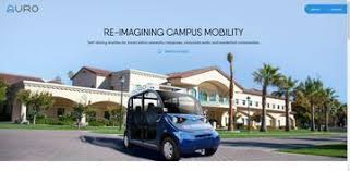
Today’s announced acquisition of Auro Robotics by RideCell should go a long way toward clearing things up. RideCell has announced today its all stock acquisition of Auro Robotics, maker of driverless, zero-emission shuttles.
Auro’s SAE Level 4 application of geo-fenced automated driving is precisely what is at stake in the current debate: self-driving shuttles operating in a defined area. Of course we’ve seen the headline-grabbing antics of Tesla Motors’ Level 2 vehicles and Waymo’s Level 4 shuttles with human operators, but Auro is first to market with a commercial driverless application.
Simultaneous to its acquisition of Auro, RideCell also announced the public availability of its autonomous operations platform which has been used in multiple autonomous pilot programs. Ridecell now offers the industry’s first complete autonomous new mobility solution that enables on-demand autonomous shuttle mobility service in low-speed, private-road settings.
While testing on public roads, including highways and surface streets, and in dense urban environments may represent brass ring objectives for the autonomous driving industry, controlled use opportunities represent the low hanging fruit that will pay the bills and pave the way. The Auro acquisition allows RideCell to accelerate the evolution of its connected autonomous vehicle platform while enabling the company to refine the critical user interfaces crucial to crafting real world applications.
RideCell may have 20 customers operating in a variety of environments and scenarios, but the Auro acquisition and the new autonomous platform opens the door to opportunities where vehicles may or may not already be implemented. While RideCell partners, such as BMW’s ReachNow, may be operating in the wild with human drivers accessing car sharing or ride hailing use cases, the stage is set with Auro for a future driverless ReachNow proposition.
RideCell says it will continue to collaborate with partners to apply the RideCell platform to self-driving vehicles for automated management of operational tasks including cleaning, refueling, and emergency response situations. Auro expands RideCell’s opportunities with shuttle manufacturers to add self-driving capabilities for neighborhood electric vehicle platforms. These systems are designed to safely drive people around campuses, theme parks, resorts, business parks, and retirement communities.
Private environments with low-traffic, low-speed roads provide the perfect setting for deploying autonomous vehicles today. Auro-enabled shuttles were among the first driverless shuttles put into daily operation on the Santa Clara University campus in California and have already provided safe transportation to thousands of riders, the companies say.
The future of self-driving cars, therefore, is unfolding on college campuses, in theme parks, at resorts and in retirement communities. These are the places where valuable human interactions will be tested and assessed for the refinement of systems which will ultimately be accessible on surface streets, in urban centers and on highways. This is how we autonomous. This is why we autonomous.