Last week saw a unique confluence of events that continue the negative news flow in semicap following the story about GloFo. At a financial conference, Micron’s CFO said NAND prices were declining, this was on top of an analyst note in the morning about the same issue. Even though this should be no surprise as memory has had an overly long strong run.
Then KLAC’s CFO tempered expectations for the balance of the year due to the pushout of DRAM business that was already announced and well known in the industry. (Samsungs pushout of spending..)
Also read: GLOBALFOUNDRIES Pivoting away from Bleeding Edge Technologies
Separately either topic is well known and out in the public domain already but being “announced” at the same time in the first conference back from the summer sets an ominous tone, and acts like a catalyst.
Micron announcing declining NAND prices is like pouring gasoline on the already dry tinder of memory concerns then ignited by a cigarette flicked out the window by KLAC’s comments.
We now have a meltdown…..even though its not a lot of new news and things we have been talking about for a long time….
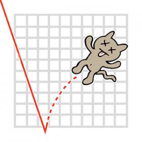
Dead Cat Bounce Done?
Concerns about memory seem to have faded over the summer during vacations when the market is usually quiet but the issue never really went away. We have been very clear that the memory run was too strong for too long and well overdue for a correction that we had already started to see months ago.
Falling NAND pricing or DRAM pricing should be no surprise but perhaps having multiple comments on the first day back are a bit too much…..
Stock had recovered a bit while investors took their eye off memory concerns and we had a little bit of a dead cat bounce but now it sounds like multiple doctors are declaring the cat truly dead…….
Q4 “Snapback ” not so “Snappy” now
While the vast majority of analysts and bulls on the stocks rushed out in support of a one quarter downturn, we took a more conservative view suggesting we were very “dubious” as it would make absolutely no sense for Samsung to push out only one quarter. It now seems our more conservative view may be borne out as we are now talking about 1H19 recovery (maybe…). While CQ3 may still be the “trough”, but the length of the trough and the angle of recovery out of the trough is more questionable.
GloFo not that impactful..
The reality of last weeks news about GloFo dropping out of the 7NM race while surprising is not hugely impactful on the revenues of semicap companies. The reality is that most tool makers had long ago discounted GloFo as a major player and discounted the revenue expectations from them. The real issue is more the view that it is additional negative news and the ability to make up for a memory shortfall from the foundry side all that much more difficult.
So while the GloFo news itself is not that negative, its when its taken in context with the overall negative news flow we are experiencing.
KLAC bulletproof vest weakened
KLAC’s “defensive” play ,which up until now has been working, is obviously taking a bit of a hit. KLAC’s stock which has held up way better than AMAT & LRCX due to its lower memory exposure is now leading the group lower today. This lower memory exposure premium the stock has enjoyed will obviously be reduced now that the same memory issue is impacting KLAC’s financial performance.
To be clear, KLAC still has much less memory impact than AMAT or LRCX, but it does not have zero impact. The foundry side of KLAC’s business is unaffected and still very strong.
The stocks
Today is an ugly wake up call after a relatively quiet semiconductor summer. There is not a lot of new news here but putting it all together in one place and time is obviously overwhelming the stocks.
We have been very clear, for a long time, that memory was too strong for too long, and had to cool off. Wether it cools slowly or takes polar bear plunge matters little. It actually may have been better for memory to drop quickly and get it over with rather than reliving the fear of memory pricing dropping over and over again.
Likewise with the semicap stocks, its time to get over the fact that the industry is still cyclical and goes up and down. Customer concentration is making that worse. It is also naive to assume only a one quarter, or one company, slow down. All the cyclical downturns we have seen have more than one negative issue.
We had said that AMAT had downside to the low $40’s and we are there. We had also said that LRCX could have downside to $150ish but we are still a bit above that. KLAC may have lost about a 10% premium that it has held as a “defensive” play.
Micron is very, very cheap and getting cheaper. The negative memory discount has been applied too many times as the company is still making a lot of money.
We probably have another 6 weeks or more until companies report and we get a sigh of relief as fears turn into reality which is usually less negative than the anticipation itself.
In the meantime we find it hard to catch a falling spear and buy into this continuing flow of negative news especially given the skittishness of the overall market.