As new automotive Advanced Driver Assistance System (ADAS) based product releases intensifies while a more stringent set of safety requirements are mandated, it is not surprising that subsystem and electronic suppliers are looking for pre-designed and ISO 26262 certified IP that can address both imperatives of schedule and safety when being integrated into SoCs. Add to that the necessity of lower power and higher performance, you begin to look at newer architectures that minimize footprint, risk, and effort and maximize the performance at the same time.
Traditionally, the electronic control units (ECUs) for individual ADAS applications have been placed throughout the car: the forward collision avoidance ECU located in the windshield, park assist ultrasonic sensors, and the processor in the rear. ECUs integrate the multiple ADAS applications into centralized domains to combine multiple ADAS functions. The new class of integrated domain controller ECUs utilizes data transferred from the car’s remote sensors such as cameras, LIDARs, radar, ultrasonic, and other sensors to the integrated domain controller for processing by a high-performance ADAS system-on-chip (SoC).
The IP in the integrated ADAS domain controller SoC must also meet the highest Automotive Safety Integrity Levels (ASILs), must be designed and tested for grade 1 and 2 temperatures, and must fully adhere to the automotive quality management process. In addition, to meet the power and performance requirements of the new integrated ADAS domain controller SoC architecture, designers are moving to more stringent process technologies, such as FinFETs, making it even more important to use automotive-certified IP in advanced foundry processes.
A Shift to Integrated ADAS Domain Controller SoC Architectures
According to the August 2016 Traffic Safety Facts Research Noteby the National Highway Traffic Safety Administration (NHTSA), “the nation lost 35,092 people in crashes on U.S. roadways during 2015, a 7.2% increase which is the largest increase in nearly 50 years.” It was analyzed that about 94% of those accidents were caused by human error, and the rest by the environment and mechanical failures.
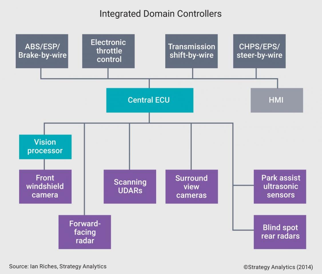
The opportunity to reduce car accidents is making automotive ADAS even more critical. Automatic emergency braking, pedestrian detection, surround view, park assist, driver drowsiness detection, and gaze detection are among the many ADAS applications that assist drivers with safety-critical functionalities to reduce car accidents. Figure 1 shows an integrated ADAS domain controller SoC with a centralized ECU where data from numerous sensors travels to a central ECU and is then processed via an ADAS processor.
Figure 1: Data from sensors travel to a central ECU and are processed via a vision processor
High volumes of data are driving the adoption of 64-bit processors for automotive ADAS applications. The shift from a distributed architecture to a more centralized ECU is more prevalent, and since the ECUs are integrated, the ADAS SoCs are becoming very complex, requiring the latest semiconductor features, semiconductor process technologies, along with other technologies for ADAS domain controller SoCs:
- Ethernet manages high data volume including time-sensitive data and reduces point-to-point wiring
- LPDDR4/4x operates at data rates of up to 3200 megabits per second and beyond, which speeds up the DRAM operations in automotive-grade SoCs
- MIPI standards like MIPI Camera Serial Interface and Display Serial Interface provide high-performance connectivity in imaging and display applications
- PCI Express has high-reliability processor-to-processor connectivity for 4G radios or the future 5G radios and external SSDs
- 5G and IEEE standards, like 802.11p, help provide real-time updates of maps or images to and from the Cloud, and vehicle-to-vehicle or vehicle-to-infrastructure communications
- Security protocols in hardware and software for data protection to and from connectivity via USB, WiFi or Bluetooth
- Sensor and control subsystems offload the host processor and fuse sensor data to manage the different type of sensor data provided by the sensors
- More advanced manufacturing process technologies from the traditional 90-nanometer (nm), 65-nm and 40-nm to more advanced 16-nm, 14-nm, and even 7-nm FinFET processes
Safety-critical applications are significantly increasing the adoption of ADAS SoCs. However, it is required that the ADAS SoC along with all semiconductor components including the IP that is integrated into the SoC meet the ISO 26262 functional safety standard.
Meeting ISO 26262 Functional Safety Standard Requirements
ISO 26262 is a standard that defines the impacts of failures in automotive systems at four different Automotive Safety Integrity Levels (ASILs): A, B, C, and D; ASIL D is the highest level of functional safety. The ISO 26262 standard defines all the processes, development efforts, and standards that automotive development organizations must implement and comply with when developing products for safety-critical systems. A key objective of ISO 26262 standard is to minimize the susceptibility to all types of random hardware failures, including permanent failures or transient failures, by:
- Defining the functional safety requirements when developing products
- Applying rigor to the development process
- Defining a safety culture
- Implementing safety features to minimize the impact of hardware failures
- Assessing and analyzing the impact of safety features to ensure mitigation of hardware failures
Industry-accredited inspection companies, such as SGS-TUV Saar, are available to audit products and processes for compliance and certification of ISO 26262.
The ISO 26262 certification process includes multiple steps, policies, and reports and must start from the very beginning of product development. For example, the Failure Mode Effect and Diagnosis Analysis (FMEDA), a report that development teams generate, provides all the information regarding the adherence to ISO 26262 from a functional safety perspective.
Created by design and verification engineers, the report is a critical component of an ASIL assessment, not just for evidence of compliance but also for design targets and a rating assessment at the end of the development flow. Designated safety managers, separately from the development organization, who are fully trained to monitor the development process, milestones and product reviews, ensure all the documentation and traceability is completed throughout the SoC development flow as defined by the standard.
The FMEDA report also includes a summary of the safety features, their development, and verification. It clearly documents the safety features contained in the products and how these products react to the random faults that are injected into them. The FMEDA report is mandatory and is given to all parties involved in the product review process.
How ISO 26262 Certification is Implemented
A standard SoC or IP product development flow starts with register-transfer level (RTL) design, which is then implemented, verified, and validated in hardware and software in the final prototypes. An ISO 26262 compliant development adds additional steps over the standard design process including at the very start when defining a core architecture and specification. Designers define a safety plan that includes safety features and goals. The product team and safety manager review the safety plan and strategy to achieve the designated functional safety for the end application.
It is important to conduct a failure analysis by injecting faults to assess the safety level and the system’s reaction to those faults. The FMEDA shows a fault injection analysis for both permanent and transient faults to assess the impact. The analysis and assessments are clearly documented in the FMEDA report as part of the ISO 26262 certification process along with the safety manuals. This entire process is shown in Figure 2.
Figure 2: An example of a standard SoC or IP design with additional ISO 26262 certification steps and requirements
The safety manual in the ISO 26262 certification process defines the safety features in the product, which is critical to the operation of the product. The standard provides some guidelines as to the effectiveness of safety features that can detect possible failures. Safety features for IP product design fall into three categories: protection mechanisms, replication, and various.
- Protection mechanisms, such as protecting the interface between the IP in the SoC architecture with the protection of elastic buffers, parity protection on the data path and configuration registers, and error correction code protection for both writes and reads.
- Replication is a safety feature category that includes duplicating (or triplicating) key modules and using voting logic to ensure redundancy.
- Various includes parity checks for all the state registers, single cycle pulse validity, various dedicated interrupts, and hot state machine protection for bad states.
The process to meet ISO 26262 functional safety certification is stringent from creating the FMEDA report, designating a safety plan that defines safety features for the target ASIL, to employing a safety manager and documenting and reviewing every milestone with all the stakeholders. In addition to meeting ISO 26262 functional safety requirements, integrated ADAS domain controller SoC development teams and the rest of the supply chain, including the design IP provider, must adhere to automotive reliability and quality requirements.
To meet the automotive reliability standard as defined by the automotive industry, automotive SoCs and IP must be designed and tested to meet very low defect densities which are measured by Defects Parts Per Million (DPPM). The automotive industry has a requirement for less than one DPPM, encouraging designers to set a goal of zero defects per million throughout the automotive product lifetime of 15 years.
Meeting temperature grade is another reliability requirement. For ADAS, the highest level of operating temperature is Grade 1 which requires up to 125 degrees Celsius ambient or 150 degrees Celsius junction temperatures. Each company within the automotive supply chain has a proprietary temperature mission profile to which they design and test their products. SoC and IP designers who are developing products for the different ADAS applications take the temperature mission profiles into account during the development process. Different requirements such as electromigration, transistor aging, and transistor self-heating must be considered against the temperature mission profile for the different devices.
Synopsys offers a portfolio of automotive-certified IP that is ASIL Ready ISO 26262 certified, designed, tested for grade 1 and 2 temperatures, and fully adhere to the automotive quality management process. For information view the DesignWare IP for automotive SoC web page.Based on a technical bulletin posting By Ron DiGiuseppe, Automotivie Segment Marketing Manager, Synopsys