RVN! 26 Banner revised (800 x 100 px) (600 x 100 px)

SPIE Advanced Lithography Conference 2019 Overall Impressions

SPIE Advanced Lithography Conference 2019 Overall Impressions
by Scotten Jones on 03-05-2019 at 6:00 am

Last week I attended the 2019 SPIE Advanced Lithography Conference. I gave two presentations, attended dozens of papers and conducted three interviews. I will be doing some detailed write ups particularly on EUV but I am waiting for the presentations from several of the papers. In the mean time I thought I would put some overall impressions together.


Canon event

The conference began for me on Sunday morning at a Canon private briefing for about 50 customers and partners where I was an invited speaker. One of the other speakers was Yan Borodovksy, a former senior fellow at Intel (Intel’s highest technical level), now retired and a fellow of SPIE. Yan made what I thought was the funniest comment of the entire week. He basically said, “Moore’s law isn’t dead, it just had a stroke and stopped moving on one side”.

Nikon LithoVision
Where the Canon event was private and limited to customers and partners, Nikon’s LithoVision is a more public event attended by over 500 people. I was also invited to speak at LithoVision and I have written my talk up here.

My favorite talk of the event was Anton Devillier’s animated and entertaining talk about what he would tell lithographers if he could go back in time. He had a very cool illustration of a worm hole and talked with so much energy that at one point his lavalier mic went flying.

Overall Conference
I thought the overall conference was relatively quiet this year. Last year was as Chris Mack put it, “The year of Stochastics” where it seems everyone had just woken up to the idea that we had to actually make EUV work and now had to face the practical problems. This year to me was much more a year of quiet progress and continuing investigation.

My impression was ASML and Imec were the key presenters this year providing a lot of the material. Imec alone was first author on 32 papers and coauthors on even more

There was a lot of papers on EUV against the background that after many years waiting for implementation, that EUV is actually ramping up in production now.

The following isn’t specific to the conference but sets a background on EUV.

Samsung is currently ramping up a 7nm EUV based foundry logic process with approximately 7 EUV layers including what we believe to be a 36nm metal pitch printed with EUV. TSMC has been in production with their optical 7nm 7FF foundry logic process since last year and is now ramping their 7nm 7FF+ process with 5 EUV layers. We believe the minimum EUV pitch on 7FF+ is 40nm. The word out of TSMC is that the process is going very well including the performance of EUV. Later this year TSMC is expected to begin risk starts on a 5nm foundry logic process with more extensive EUV usage. We believe the 5nm process will include 28nm minimum metal pitches produced by EUV. Once again, the word out of TSMC is this process is going very well including EUV. Intel is also working on EUV for their 7nm process due in 2020. EUV is clearly ramping into high volume manufacturing and by all accounts the implementation is going well.

ASML
ASML provided updates on the current 0.33 NA systems and the 0.50 NA (high NA) system in development and I sat down and interviewed Mike Lercel (Director of Strategic Marketing) as well. I will provide a more detailed write up on these systems once I get the ASML presentations. A few initial observations:

[LIST=1]

  • There are now 40 EUV systems in the field representing proximately $4 billion dollars of investment by device manufacturers.
  • ASML is expected to ship 30 EUV systems this year (some Q1 shipments may already be in the 40-system number) and 40 more EUV systems next year. That represents approximately $3B and $4B of additional investment for 2019 and 2020 respectively.
  • ASML will begin shipping the NXE3400C system later this year with improved uptime and throughput.
  • The High NA system design is well underway and ASML and Zeiss (the lens manufacturer) are expending their facilities in preparation for production.

    Imec
    Imec presented work in multiple different areas and I also had the opportunity to interview Greg McIntyre (Director of Advanced Patterning), John Peterson (Principle Scientist) and Yasser Sherazi (R&D Team Leader for Design). I will be doing a detailed write up of the Imec work once I get the presentations from them.

    [LIST=1]

  • John Peterson gave an interesting talk that showed just how little we understand how EUV photoresist works, Imec along with KMLabs has announced a new lab to study reactions in EUV photoresist in the attosecond to picosecond range (E-18 to E-12 second range).
  • Imec has identified cliffs in the EUV photoresist process where on the low CD side there is an exponential increase in micro birding or missing contacts and on the high CD side there is an exponential increase in broken lines and merging contacts. New at this year’s conference was characterization of a defect noise floor between the two cliffs. The noise floor was around E-7 in one experiment and then improved to around E-8 with a different photoresist and complex filtration. I asked John Peterson whether these limits were fundamental. He said that for an 80mJ/cm2 dose the photo shott noise limits was approximately E-11 so we are no where near the limit yet.
  • Imec also present work on sequential infiltration synthesis (SIS) that provides smoothing and improved etch resistance of EUV photoresists.
  • There were several Imec papers on design improvements. Buried power rails and backside power distribution are powerful scaling boosters. Device architectures such as CFETs can drive cell heights all the way down to 3 tracks.

    Veeco
    EUV uses complex multi layers reflective masks, the absorber pattern on the mask surface has a thickness that can lead to 3D shadowing effects at small feature sizes and or larger incident radiation angles such as what we will see with high NA EUV systems. Veeco make deposition and ethc tools used to make EUV masks and they are involved in work to change to high-k absorber materials enabling thinner absorber films. I interviewed Meng Lee (director of product marketing) about etching of hig-k materials.

    Summary
    In summary, there was a lot of interesting up-dates on EUV systems and processing as well as new design technique to enable future scaling. I will be writing this up in detail over the next couple of weeks so keep your eye on SemiWiki for my articles.

    Also read: LithoVision 2019 – Semiconductor Technology Trends and their impact on Lithography


  • GLOBALFOUNDRIES UPDATE 2019

    GLOBALFOUNDRIES UPDATE 2019
    by Daniel Nenni on 03-04-2019 at 12:00 pm

    The GLOBALFOUNDRIES story has been one of the more interesting ones inside the fabless semiconductor ecosystem. It started in 2008 when AMD announced a partnership with ATIC of Abu Dhabi to create a new joint venture company to become the world’s first truly global semiconductor foundry. On March 4[SUP]th[/SUP] of 2009 (happy birthday!) GLOBALFOUNDRIES was launched and the rest as they say is history. It has been an exciting story to cover. Thus far we have published 189 GF related blogs that have been viewed more than 2,879,504 times and the story is far from over.

    Recently rumors of GF being up for sale have been reported by media outlets desperately seeking semiconductor clicks. In my opinion the reports are FALSE but it is certainly something worth discussing. First a little semiconductor insider perspective:

    GF had a rough start due in part to a shift in the foundry landscape. TSMC made a series of technology changes that made it difficult for others to follow. It all started at 28nm. While most foundries chose the gate-first implementation TSMC chose gate-last. As it turned out the gate-first implementation did not yield properly which gave TSMC their largest process node lead ever. UMC and SMIC ended up changing to gate-last to copy TSMC and get second source manufacturing market share but Samsung and GF stayed with gate-first. Then came FinFETs which made following TSMC for second source business impossible. Samsung did a very nice job with 14nm which resulted in a 50/50 split market share with TSMC 16nm but TSMC quickly came back with 10nm and 7nm and is now in a dominant foundry position.

    This caught GF in between two fierce competitors (TSMC and Samsung) which is an impossible place to be in the foundry business, even for a chip giant like Intel. The end came last year when both Intel and GF decided to step aside and let TSMC and Samsung battle for the leading edge foundry business. The GF pivot is still in process and it does include asset sales thus the rumors.

    If you look at GF there are five different semiconductor units if you will: Singapore fabs, Dresden fabs, the Malta fab, IBM fabs, and the new fab in China.

    One of the Singapore fabs (MEMs Fab 3e) has already been sold to VIS in Taiwan. TSMC is a major shareholder in VIS in case you did not know. From what I have heard the other Singapore fabs are also for sale. In my opinion they will be sold to an Asian semiconductor company. I see no future for GF in the bulk CMOS business and it is best to sell the cow while it still has milk.

    The other GF fabs have significant government funding and other entanglements so their sale will be much more complicated.

    The Malta fab has NY State money and is currently running Samsung 14nm technology so I only see Samsung as an acquisition candidate. Samsung already has a fab in Austin, Texas but adding another fab in NY would not be a bad thing for US foundry customers. It is also possible for GF to migrate Malta to FD-SOI when extra capacity is needed. From what I am told it would not be that big of a jump.

    The Dresden fabs are probably the most desirable since they are leading edge FD-SOI but again government money is involved. If the German Government was forward looking they would take an active role in their semiconductor future and embrace GF Dresden, but probably not. Even so, I see Dresden as being the jewel in the GF fab crown moving forward. Especially now that GF has reportedly moved advanced mask making tools from Vermont to Dresden. The China fab in Chengdu is also FD-SOI so I would put it right next to Dresden in the crown jewels.

    Last but not least, the IBM fabs (Essex Junction and Fishkill) also have complicated government entanglements as well as being trailing edge so I see no acquisition opportunities there. In my opinion they will die a slow and profitable death as many US fabs have before them.

    Bottom line: I do not see GF being sold off. On the contrary, I see GF consolidating into a worldwide FD-SOI powerhouse, absolutely.


    Radar is Cheaper but Autonomous Car Needs Lidar!

    Radar is Cheaper but Autonomous Car Needs Lidar!
    by Eric Esteve on 03-04-2019 at 7:00 am

    To replace a human driver, autonomous car will have to “see” and do it in a better way than human being. The available solution, based on camera, radar, lidar, is not perfect and need to be improved. Radar is great for “seeing” in bad weather but has insufficient resolution to distinguish distant objects. Lidar produces high-resolution images but is unreliable in bad weather. A combination of two could be attractive, unfortunately the lidar cost (in the several $1K range!) is way too expensive to deploy the technology in autonomous driving to have a chance to penetrate the broad automotive market.

    Engineers are working hard to propose drastic cost reduction and shrink for lidar and to develop higher resolution radar. Using solid-state and MEMS technology in lidar will help lower cost and reduce size, while radar is moving toward higher resolution “imaging” radar through more antennas and 4D.


    The Cadence/Tensilica DSP based solution, is able to run lidar sensor pre-processing and processing in order to provide sensor data to be analyzed through neural network and machine learning included in the DNA processor family, and finally decision to support driver assistance.

    This “philosophy” should allow to develop more affordable lidar and most efficient radar in the future and help democratize autonomous car. Cadence/Tensilica offers a broad range of Application-Specific DSPs supporting radar, lidar, 5G, 4G/LTE-A, bluetooth, smartgrid, and 802.11 modems. Based on a deeper processor pipeline architecture, the ConnX B20 DSP provides a faster and more power-efficient solution for the automotive and 5G communications markets—including next-generation radar, lidar, V2X, UE/infrastructure and IoT applications.

    There are three main sensors required going forward: cameras, radar and lidar. Cameras use visible light and rely on any objects they wish to see being illuminated. Radar and Lidar sensors emit (modulated) electromagnetic waves that reflect off objects and are then detected back at the sensor. The “R” in Radar is for Radio, the “L” in Lidar is for Light.

    Radar sensors emit millimeter waves that work well in poor weather conditions and at long distances as the waves are not easily attenuated in the atmosphere. However, although they are small and low cost, today they are not able to produce a high-resolution image at a distance that can distinguish between multiple objects – something that lowers the safe speed for AD if relied upon for object detection. Radar manufacturers are now developing “imaging” or ”4D” radar solutions that provide much higher resolution from the use of more antennas and much more digital signal processing.

    Lidar sensors emit nanometer waves (laser beams) and is a surveying method that measures distance to a target by illuminating the target with pulsed laser light and measuring the reflected pulses with a sensor. Differences in laser return times and wavelengths can then be used to make digital 3-D representations of the target.

    Imaging lidar can be performed using arrays of high-speed detectors and modulation sensitive detector arrays typically built on single CMOS chips. In these devices each pixel performs some local processing such as demodulation or gating at high speed, down-converting the signals to video rate so that the array can be read like a camera. Using this technique many thousands of pixels / channels may be acquired simultaneously. High resolution 3-D lidar cameras use homodyne detection with an electronic CCD or CMOS shutter.

    In 2014, Lincoln Laboratory announced a new imaging chip with more than 16,384 pixels, each able to image a single photon, enabling them to capture a wide area in a single image. The chip uses indium gallium arsenide (InGaAs), which operates in the infrared spectrum at a relatively long wavelength that allows for higher power and longer ranges. In many applications, such as self-driving cars, the new system will lower costs by not requiring a mechanical component to aim the chip.

    In conclusion, when the industry will be able to get rid of electro- mechanical component and move to CMOS MEMS devices, it will be possible to broadly integrate Lidar technology in the automotive industry. Benefiting from high performance DSP IP will also be key to enable low cost processing to support Lidar, that’s the goal of Cadence/Tensilica ConnX B20DSP!


    Tensilica/Cadence ConnX B20DSP has been designed to provide significant improvements compared to the ConnX BBE32EP DSP. The B20 DSP is up to 30X faster in parts of the communication processing chain and up to 10X faster in parts of the radar/lidar processing chain.

    With deeper processor pipeline, B20DSP offers higher frequency, 1.4 GHz or greater in 16nm. The instruction-set has been enhanced and for higher accuracy, offers more floating point and forward error correction (FEC). Tensilica existing customers will enjoy software compatibility with other members of the ConnX DSP family, and new customers should enjoy easy scalability for product roadmaps and across product lines!

    Readers can get more information:
    https://ip.cadence.com/ipportfolio/tensilica-ip/comms-dsp&CMP=TIP_CnXB20_IndTre_Arti_0219_PP

    ByEric Esteve fromIPnest


    Stemming Mobility Race to the Bottom

    Stemming Mobility Race to the Bottom
    by Roger C. Lanctot on 03-03-2019 at 12:00 pm

    Pundits and pontificators are publishing viewpoints on a utopian future of smart cities and optimized transportation options populated with new mobility solutions ranging from automated ride hailing services to sharable bikes and scooters. In this halcyon view, the bikes and scooters and ride-hail cars will deliver passengers to public transit hubs while privately owned vehicles are prevented from entering the city center.

    The stated objective of most of these operators, and their visionary supporters, is to separate people from car ownership. This goal is looking increasingly unlikely as frustration with these emerging alternatives grows and undermines the quality and reliability of the legacy solutions they seek to replace.

    Ride hailing and bike and scooter sharing operators have opened a massive financial sinkhole in the middle of what was once a profitable industry built around ad hoc transportation options. In the process, these new operators have unleashed a race to the bottom endangering the quality of service for all while compounding traffic and emissions challenges for the public.

    Ride hailing service providers from Grab to Gett to Yandex, Lyft and Uber are piling up billions of dollars in losses and looking to the public markets to bail them out. Bike and scooter sharing operators are cannibalizing one another’s businesses in a loss-producing tornado while complicating both pedestrian and vehicle traffic in most cities.

    In the midst of this mobility maelstrom the busses, trams, taxis and subways plod on amidst a rising tide of Ubers and Limes and Birds jamming up streets and sidewalks and eroding revenues. Even Amazon has contributed to the mobility malaise with delivery vehicles parking hither and yon dropping off packages that might otherwise have arrived via existing postal services.I

    nto the breech strides New York City. Widely perceived as having driven away Amazon and its HQ2 plans for Long Island City, the city is seen as a potential paragon standing in the path of e-commerce and mobility monopolists, Amazon and Uber.

    In addition to spiking Amazon’s plans, NYC has capped the number of Uber drivers and may well do worse, in an effort to preserve transportation equity while preventing the status quo from deteriorating into ad hoc mayhem. NYC is not alone. Cities elsewhere in the world have either outright banned Uber for failing to do sufficient driver background checks or other certifications or have instituted discriminatory taxes to slow the onset of freelance ride hailing by non-professional drivers.The early promise of bike share operators such as LimeBike has deteriorated in the face of emerging scooter share companies. Where bike sharing might have forged a path to profitability, unprofitable scooter operators are stealing away customers jeopardizing both business propositions.

    Lime has taken to expanding its portfolio to scooters and shared cars in a desperate stab at shoring ups its eroding market leadership and establishing some bona fide profitability in its operations. Most notable in Lime’s move is its introduction of car sharing – a clear indication that car sharing – unlike “ride sharing/hailing” – is perceived as a profitable model.

    It’s becoming clearer, now, that cities will have to step forward to pick winners in this process of evolving transportation. Survival of the fittest is an unfit model for optimizing transportation options.

    For New York City, 2019 is increasingly perceived as the year the political dam breaks and the local government, with the blessing of the state, turns to congestion charging. Cities like London and Stockholm have already taken that step.

    What if every city required Uber/Lyft/Gett/Grab/Yandex/etc. to include local taxi providers in their apps as a prerequesite to gaining a local license? I’d be shocked if that hasn’t been tried and a growing roster of app providers from HERE Mobility to Splyt are already doing so. In fact, some ride hailing companies have already partnered with taxi operators outside their operating home base.

    The real change this year will come from cities embracing this challenge and bringing together internal constituencies – bus, rail, tram and subway transit leaders, taxi and limousine regulators, bridge and tunnel operations, the public – to gather the relevant data and meet the challenge head on. The challenge of moving people within existing finite infrastructures cannot be solved by free enterprise alone and the fixation on convincing consumers to abandon car ownership must be set aside.

    Finding fair, equitable solutions will be no easy task. The ultimate goal is livability including reducing emissions, increasing vehicle and pedestrian throughput and reaching zero roadway fatalities. The formula will vary from city to city and profitable operations should be a key criterion.


    No Cord Cutting Autonomous Cars

    No Cord Cutting Autonomous Cars
    by Roger C. Lanctot on 03-03-2019 at 7:00 am

    The automotive industry is a world of contradictions. Nowhere is this more evident than in the realm of connected cars. Car makers remain utterly conflicted over connecting cars 21 years after General Motors got the ball rolling with the introduction of OnStar.

    Even GM had to famously be goaded into connecting its cars by then executive vice president and general counsel, Harry Pearce, who touched off what became known as Project Beacon by rhetorically asking a collection of GM executives: “Now, how many out of a hundred OnStar-equipped cars that crash will need to call for help before we’d be more wrong for holding back a potentially lifesaving technology like this than we would be for putting it in?”

    February 2019 finds the industry on the precipice of a world where the embedded wireless connection in the car will not only be able to summon assistance in the event of a crash a la OnStar, but will soon be able to help the car and driver avoid a crash altogether. It is for this reason that forecasters like my employer Strategy Analytics foresee an acceleration in the adoption of automotive wireless technology.

    This proposition is especially relevant on the eve of Mobile World Congress in Barcelona – where multiple car companies will exhibit and connected and autonomous cars will be demonstrated. Yet, many automotive engineers continue to aver that wireless connectivity is non-essential for the operation of autonomous vehicles.

    It is easy to see the source of this misguided perspective given that autonomous vehicle tech leaders such as Waymo, Tesla Motors, Nvidia and Intel/Mobileye all tend to downplay the role of connectivity. These companies need look no further than GM’s Cruise Automation to see a semi-autonomous vehicle aggressively leveraging wireless technology

    General Motors integrates wireless connectivity in both the Cruise Automation platform and its Super Cruise advanced cruise control system. The Cruise Automation car comes with simultaneous connectivity to four wireless carriers. The Super Cruise system, currently only available in select Cadillacs, supports only one carrier.

    The significance is that both systems make use of connectivity to enhance contextual awareness and vehicle positioning. Today, these two implementations are something of a belt-and-suspenders approach to automating driving. Soon, wireless connectivity for autonomous vehicles will be required.

    This is why the resistance to wireless connectivity for autonomous operation at companies like Volkswagen is so mystifying. A budding recognition is sweeping the automotive industry that the onset of cellular C-V2X technology in advance of the rollout of 5G is radically changing the notion of connecting cars.

    The industry has rapidly shifted from OnStar-like automatic crash notification (in the event of a collision) to a focus on on-board Wi-Fi connections to the integration of digital assistants and, finally, wireless enabled and enhanced autonomous operation. If there is any remaining doubt at large auto makers – such as VW – that connectivity is key to autonomy one need only consider the future requirement for remote vehicle control.

    Finland’s regulators, for example, have stated that autonomous vehicles must have human drivers, but those drivers need not be in the vehicles. Finland is not alone. Regulators across the world will swiftly grasp that remote control is an essential element of autonomous operation (in the event of system failure or malicious intrusion) and 4G/5G-style connectivity will be essential to deliver this solution.

    Remote control of autonomous cars will require 4G/5G connectivity and 4G/5G connections will help enable autonomy. The low latency, mesh networking, edge computing and vehicle-to-vehicle communication characteristics of 5G will accelerate autonomous vehicle development.

    Car companies as a whole are far from “cutting the cord.” Car companies are adding redundancy to their wireless connections. Dual SIM Dual Access (DSDA) and three- and four-SIM vehicles will arrive in the market by the end of 2019.

    Cars will increasingly be connected, whether they operate autonomously or semi-autonomously. Remote control or tele-operation will dictate that car makers have an improved sense of the reliability of the wireless connection to their vehicles. Companies like Phantom Auto, Designated Driver and Ottopia have already emerged to meet this requirement.

    Quality of Service requirements for connected cars, autonomous or otherwise, is radically changing the thinking of automotive engineers. In many ways, though, the thought process remains the same.

    As OnStar’s first president, Chet Huber, noted in his book “Detour:” “…his (Harry Pearce’s) standard was clear. We would need to do everything we knew how to do to make it as reliable as best-in-class technology and strong operating discipline made possible.” In other words, car makers across the world have come to recognize that a single SIM may not do the trick.

    Connecting cars isn’t about automatic crash notification or Wi-Fi or digital assistants. Connected cars of the future will leverage their connectivity to avoid crashes and save lives and that will require a reliable connection.

    Roger C. Lanctot is Director, Automotive Connected Mobility in the Global Automotive Practice at Strategy Analytics. Roger will be chairing the 5GAA event Wednesday, Feb. 27, at Mobile World Congress in Barcelona and participating in the Future Networked Car Workshop, March 7, at the Geneva Motor Show – https://www.itu.int/en/fnc/2019. More details about Strategy Analytics can be found here: https://www.strategyanalytics.com/access-services/automotive#.


    LithoVision 2019 – Semiconductor Technology Trends and their impact on Lithography

    LithoVision 2019 – Semiconductor Technology Trends and their impact on Lithography
    by Scotten Jones on 03-01-2019 at 12:00 pm

    I was asked to present at Nikon’s LithoVision event again this year. LithoVision is held the day before the SPIE Advanced Lithography Conference also in San Jose. The following is a write up of my talk.
    Continue reading “LithoVision 2019 – Semiconductor Technology Trends and their impact on Lithography”


    Report from SPIE EUV Update 2019

    Report from SPIE EUV Update 2019
    by Robert Maire on 03-01-2019 at 7:00 am

    Not as much new – No breakthrough announcements, 300 watts is better than 250 watts – Pellicle Problems, TSMC is EUV king – Third times a charm? We attended this years SPIE Lithography convention in San Jose as we have for many years. Although the show was quite enthusiastic and EUV was the central topic, as it has been for a long time, there were no real “breakthrough” announcements or changes that we have seen previously.

    300 is more than 250
    It seems that ASML has had good luck and good results with it latest EUV source as it seems capable of 300 watts rather than the 250 watts specified, a nice step on the way to the needed wafer throughput

    Pellicle Problems
    On the other side of the coin, there has not been any significant progress on the transmission efficiency which is still stuck at 83% or so rather than the 90% previously hoped for. There is some discussion of carbon nanotube pellicles being worked on by IMEC but nothing real yet. Pellicles need to get better to improve throughput.

    TSMC is big man on EUV campus
    We have heard that TSMC is taking between 18 and 20 of ASML’s planned 30 EUV systems to be produced in 2019. This is a huge 180 degree reversal from a company that said they would never use EUV just two short years ago. We have heard that Intel may be good for another half dozen EUV tools in 2019 with Samsung or others taking the balance. ASML is obviously sold on on EUV for 2019.

    The risk of going “bareback”
    TSMC seems to be willing to push production without the protection of pellicles. The “print and pray” approach seems to be the way to go as there is still no mask inspection in sight, at least not from KLA. Maybe if TSMC gets paid per wafer not per known good die, they don’t care, its the customers risk. We wonder how long customers might be willing to take the defect loss from running with no pellicle. Maybe TSMC figures out how to get yield without mask inspection and never buys it by the time KLA gets it to market, probably not.

    Third times a charm
    It sounds as if the “C” version of ASML’s EUV scanner, which is now shipping, will likely be the “go to” production scanner for HVM. The “B” version which was obviously better than the prior version was better but not good enough and not economically viable for ASML whereas the “C” seems to fix all the issues (or at least enough of them) and is financially better for ASML.

    It’s party time!
    We attended both the Tokyo Electron and ASML parties at the show on Monday evening and for an industry in a slump you wouldn’t know it from the crowds at the parties nor the positive tone coming from the attendees. While there were no major new announcements at the show the tone was very positive about progress towards HVM and more layers going EUV.

    Triple patterning versus EUV
    A number of people we spoke to at SPIE suggested that the cost crossover between EUV and multipatterning was that EUV costs about the same as current triple patterning techniques. In our view, there is still a lot of room for progress in EUV costs. ASML has projected a “slam dunk” cost advantage of EUV over multipatterning but we are still not near that goal. However, EUV has power performance advantages over multipatterning that outweigh the fact that cost advantages haven’t yet been achieved. The basic fact is that EUV formed transistors are better than multipatterned transistors of the same dimensions and customers want the better product…..especially Apple.

    Impact on pricing of dep and etch
    We think that both AMAT and Lam have the opportunity to slow the move away from multipatterning to EUV by finding ways to reduce multipatterning costs. This may put pricing pressure on dep and etch tools. We think that margins at AMAT and Lam may already be under pressure as they cut pricing to get more share in a declining market as we are in. When demand has gone down in previous cycles, pricing has suffered more as the competitors have cut each others throats to get the smaller pool of business left. We have already heard of some aggressive pricing in the market that some have walked away from

    NAND and DRAM going EUV- question of when not if
    Many we spoke to at the show are already talking about when EUV will enter the memory industry. Right now there is no real reason but at some point memory will also have to go with EUV to keep up with Moore’s law…its inevitable.

    In our view this is the same question of when logic would go to EUV…..we never doubted that EUV would eventually work if enough time and money was throw at it (which it was). We think that the cost issue is a bigger impediment to EUV being used for memory production and may takes a few years to overcome. We could also hit a technology block that forces memory to go EUV before the costs come down but that doesn’t seem predictable right now

    The stocks
    We think that those investors who were worried about ASML’s EUV business in the downturn can breath a bit easier, however we can’t say the same about DUV business which will likely be impacted. AMAT and Lam still have some runway left on multipatterning given that EUV costs aren’t coming down as quickly as hoped. All in all we saw nothing at the show that made us want to go out and buy or sell a specific stock…maybe no surprises or big announcements is a good thing.

    About Semiconductor Advisors LLC
    Semiconductor Advisors is an RIA (a Registered Investment Advisor), specializing in technology companies with particular emphasis on semiconductor and semiconductor equipment companies.

    We have been covering the space longer and been involved with more transactions than any other financial professional in the space. We provide research, consulting and advisory services on strategic and financial matters to both industry participants as well as investors. We offer expert, intelligent, balanced research and advice. Our opinions are very direct and honest and offer an unbiased view as compared to other sources.


    Synopsys GLOBALFOUNDRIES and Automotive IP

    Synopsys GLOBALFOUNDRIES and Automotive IP
    by Daniel Nenni on 02-28-2019 at 12:00 pm

    IP vendors have always had the inside track on the status of new process nodes and what customers are planning for their next designs. This is even more apparent now that systems companies are successfully doing their own chips by leveraging the massive amounts of commercial IP available today. Proving once again that IP really is the foundation of modern semiconductor design.

    Automotive is one of those market segments where systems companies are doing their own chips. We see this first hand on SemiWiki as we track automotive related blogs and the domains that read them. To date we have published 354 automotive blogs that have been viewed close to 1.5M times by more than 1k different domains.


    The recent press release by Synopsys and GLOBALFOUNDRIES didn’t get the coverage it deserved in my opinion and the coverage it got clearly missed the point. Synopsys, being the #1 EDA and #1 IP provider, has the semiconductor inside track like no other. For Synopsys to make such a big investment in FD-SOI (GF FDX) for automotive grade 1 IP is a huge testament to both the technology and the market segment, absolutely.

    I talked to John Koeter, Vice President of Marketing for IP, Services and System Level Solutions. John is a friend and one of the IP experts I trust. 3 years ago Synopsys got into automotive grade IP and racked up 25 different customer engagements just last year. The aftermarket electronics for adding intelligence (autonomous-like capabilities, cameras, lane and collision detection, etc…) to older vehicles is also heating up, especially in China.

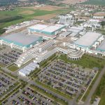
    I also talked to Mark Granger, Vice President of Automotive Product Line Management at GLOBALFOUNDRIES. Mark has been at GF for two years, prior to that he was with NVIDIA working on autonomous chips with deep learning and artificial intelligence. According to Mark, GF’s automotive experience started with the Singapore fabs acquired from Chartered in 2010. The next generation automotive chips will come from the Dresden FDX fabs which are right next door to the German automakers including my favorite, Porsche.

    One thing we talked about is the topology of the automotive silicon inside a car and the difference between central processing and edge chips. Remember, some of these chips will be on glass or mirrors or inside your powertrain. The edge chips are much more sensitive to power and cost so FDX is a great fit.

    Mark provided a GF link for more information:

    Here is the link to our Automotive resources:
    https://www.globalfoundries.com/market-solutions/automotive

    One thing Mark, John, and I agree on is that truly autonomous cars for the masses is still a ways out but we as an industry are working very hard to get there, absolutely.

    Here is the press release:

    Synopsys and GLOBALFOUNDRIES Collaborate to Develop Industry’s First Automotive Grade 1 IP for 22FDX Process

    Synopsys’ Portfolio of DesignWare Foundation, Analog, and Interface IP Accelerate ISO 26262 Qualification for ADAS, Powertrain, 5G, and Radar Automotive SoCs

    MOUNTAIN VIEW, Calif., and SANTA CLARA, Calif., Feb. 21, 2019 /PRNewswire/ —
    Highlights:

    • Synopsys DesignWare IP for automotive Grade 1 and Grade 2 temperature operation on GLOBALFOUNDRIES 22FDX[SUP]®[/SUP] process includes Logic Libraries, Embedded Memories, Data Converters, LPDDR4, PCI Express 3.1, USB 2.0/3.1, and MIPI D-PHY IP
    • Synopsys’ IP solutions implement additional automotive-grade design rules for the 22FDX process to meet reliability and 15-year automotive operation requirements
    • Synopsys’ IP that supports AEC-Q100 temperature grades and ISO 26262 ASIL Readiness accelerates SoC reliability and functional safety assessments
    • Join Synopsys and GLOBALFOUNDRIES at Mobile World Congress in Barcelona, Spain on Feb. 25 for a panel on “Intelligent Connectivity for a Data-Driven Future”

    Synopsys, Inc. (Nasdaq: SNPS) and GLOBALFOUNDRIES (GF) today announced a collaboration to develop a portfolio of automotive Grade 1 temperature (-40ºC to +150ºC junction) DesignWare[SUP]®[/SUP] Foundation, Analog, and Interface IP for the GF 22-nanometer (nm) Fully-Depleted Silicon-On-Insulator (22FDX[SUP]®[/SUP]) process. By providing IP that is designed for high-temperature operation on 22FDX, Synopsys enables designers to reduce their design effort and accelerate AEC-Q100 qualification of system-on-chips (SoCs) for automotive applications such as eMobility, 5G connectivity, advanced driver assistance systems (ADAS), and infotainment. The Synopsys DesignWare IP implements additional automotive design rules for the GF 22FDX process to meet stringent reliability and operation requirements. This latest collaboration complements Synopsys’ broad portfolio of automotive-grade IP that provides ISO 26262 ASIL B Ready or ASIL D Ready certification, AEC-Q100 testing, and quality management.

    “Arbe’s ultra-high-resolution radar is leveraging this cutting-edge technology that enabled us to create a unique radar solution and provide the missing link for autonomous vehicles and safe driver assistance,” said Avi Bauer, vice president of R&D at Arbe. “We need to work with leading companies who can support our technology innovation. GF’s 22FDX technology, with Synopsys automotive-grade DesignWare IP, will help us meet automotive reliability and operation requirements and is critical to our success.”

    “GF’s close, collaborative relationships with leading automotive suppliers and ecosystem partners such as Synopsys have enabled advanced process technology solutions for a broad range of driving system applications,” said Mark Ireland, vice president of ecosystem partnerships at GF. “The combination of our 22FDX process with Synopsys’ DesignWare IP enables our mutual customers to speed the development and certification of their automotive SoCs, while meeting their performance, power, and area targets.”

    “Synopsys’ extensive investment in developing automotive-qualified IP for advanced processes, such as GF’s 22FDX, helps designers accelerate their SoC-level qualifications for functional safety, reliability, and automotive quality,” said John Koeter, vice president of marketing for IP at Synopsys. “Our close collaboration with GF mitigates risks for designers integrating DesignWare Foundation, Analog, and Interface IP into low-power, high-performance automotive SoCs on the 22FDX process.”

    GLOBALFOUNDRIES & Synopsys at Mobile World Congress 2019
    On February 25, 2019, Synopsys will join the GLOBALFOUNDRIES NEXTech Lab Theater Session at MWC19. A panel discussion with leading industry experts, including Joachim Kunkel, general manager of the Solutions Group at Synopsys, and Mike Cadigan, senior vice president of global sales, business development, customer and design engineering at GF, will offer insights about the importance of intelligent connectivity, the growth, demands, and innovations it is poised to bring, and its impacts across the semiconductor value chain. For more information, visit:https://www.globalfoundries.com/join-gf-mwc19.

    Resources
    For more information on Synopsys DesignWare IP for automotive Grade 1 temperature operation on GF’s 22FDX process:

    About GLOBALFOUNDRIES
    GLOBALFOUNDRIES (GF) is a leading full-service foundry delivering truly differentiated semiconductor technologies for a range of high-growth markets. GF provides a unique combination of design, development, and fabrication services, with a range of innovative IP and feature-rich offerings including FinFET, FDX[SUP]™[/SUP], RF and analog/mixed-signal. With a manufacturing footprint spanning three continents, GF has the flexibility and agility to meet the dynamic needs of clients across the globe. GF is owned by Mubadala Investment Company. For more information, visitwww.globalfoundries.com/.

    About Synopsys DesignWare IP

    Synopsys is a leading provider of high-quality, silicon-proven IP solutions for SoC designs. The broad Synopsys DesignWare IP portfolio includes logic libraries, embedded memories, embedded test, analog IP, wired and wireless interface IP, security IP, embedded processors, and subsystems. To accelerate prototyping, software development and integration of IP into SoCs, Synopsys’ IP Accelerated initiative offers IP prototyping kits, IP software development kits and IP subsystems. Synopsys’ extensive investment in IP quality, comprehensive technical support and robust IP development methodology enables designers to reduce integration risk and accelerate time-to-market. For more information on Synopsys DesignWare IP, visit https://www.synopsys.com/designware.

    About Synopsys

    Synopsys, Inc. (Nasdaq: SNPS) is the Silicon to Software[SUP]™[/SUP] partner for innovative companies developing the electronic products and software applications we rely on every day. As the world’s 15[SUP]th[/SUP] largest software company, Synopsys has a long history of being a global leader in electronic design automation (EDA) and semiconductor IP and is also growing its leadership in software security and quality solutions. Whether you’re a system-on-chip (SoC) designer creating advanced semiconductors, or a software developer writing applications that require the highest security and quality, Synopsys has the solutions needed to deliver innovative, high-quality, secure products. Learn more at www.synopsys.com.


    Can I Trust my Hardware Root of Trust?

    Can I Trust my Hardware Root of Trust?
    by Bernard Murphy on 02-28-2019 at 7:00 am

    Hardware Roots of Trust (HRoTs) have become a popular mechanism to provide a foundational level of security in a cell-phone or IoT device or indeed any device that might appear to a hacker to be a juicy target. The concept is simple. In order to offer credible levels of security, any level in the stack has to be able to trust that levels below it have not been compromised. The bottom of the stack becomes the root of trust. Given the sophistication of modern threats, most of us believe that has to be the hardware itself.

    HRoTs aim to manage all security functions within a tightly-managed enclave. These would typically include functions such as secure key generation and storage, authentication, encryption and decryption and perhaps secure memory partitioning. The goal is to put all the security eggs in one basket and watch that basket very carefully rather than to scatter security features around a design and then not be sure what sneaky tricks an attacker might be able to use to get around those security measures.

    So HRoTs are a good thing. And there are quite a few vendors who have excellent HRoT IP and will be happy to have you adopt their solution. Problem solved? Not exactly. You are going to integrate an HRoT into your larger design and, sadly, there are a number of ways this can go wrong. HRoTs are configurable because one fixed design can’t fit all possible needs, and when you can configure something you can configure it incorrectly. Second, you can make mistakes in hardware connections. Don’t laugh; some of these can be very subtle. Third, and most challenging, vulnerabilities at this level are not just in hardware or just in software; they can be in a combination of hardware and software. (For those familiar with the domain, think of timing-channel attacks on cache.)

    Now you know that mistakes can happen, how are you going to find such mistakes? For the first two classes of problem, you might argue that a combination of hardware simulation and formal verification could do the trick. Maybe – problem is you first need to know what you’re looking for. But this debate is academic anyway because as soon as you need to cover hardware+software exploits, testing complexity explodes. Exploits can run over many instruction cycles and may use cache access times and other factors to accomplish their objectives. Mapping tests for any of this into standard hardware verification formats would be painful and is clearly impractical at a scale necessary to provide the comprehensive security coverage you need.

    That said, you also clearly don’t want to have to setup a whole new verification infrastructure to solve these problems. What you’d like is a mechanism which can work with your existing verification platforms, particularly emulation since you’ll want to run software on your hardware platform. A good way to accomplish this would be through a class of assertions which can capture these security level checks but then be compiled in some manner into the existing verification infrastructure.

    Tortuga Logic has created a nice approach to accomplish exactly this. I should say first that my explanation here approaches their technology bottom-up rather than a top-down presentation. But us hardware verification types may find it easier to understand. And this is just an example; talk to Tortuga for the full range of capabilities.

    Any security check really comes down to proving there is no path though which something privileged (such as an encryption key) can flow to some unprivileged location (such as a USB interface). What is a little different from pure hardware approaches is that these “things” can be logical (data in memory locations) or physical (hardware). Tortuga has a format to describe and compile this kind of assertion into your standard verification environment.

    A set of these assertions together represents a threat-model for the design; Tortuga Logic calls the language for these assertion “Sentinel”. This threat-model, together with the RTL, is compiled into a set of SVA assertions which you can run in any of your verification platforms, from formal to emulation (or even FPGA prototypes, I would guess, since they what they generate is an RTL model which runs together with your design).

    So far, so good, but many users aren’t necessarily security experts; they invested in an HRoT because they wanted to avoid becoming experts. Doesn’t this verification requirement drag them back into needing to learn more about security? Tortuga just release a new update of their software, Radix-S, which aims to put more of this verification around HRoTs on auto-pilot. Jason Oberg (the CEO) told me they have helped draft guidelines and provide more features and guidance to setup the threat model and the flow for security novices. He tells me that even the experts like this flow because for them it adds automation; they know what they want but they don’t want to have to hand-craft it every time.

    All of which is great, but for me the real deal-closer is the test-bench part of the story. Normally new simulation-based technologies can do great things only if you develop special-purpose test-benches to drive them. They sound good, but you have to do even more (and often rather specialized) test development work to tap the promise, greatly limiting their appeal. Not so with the Tortuga technology. The key differentiator in their approach is how they do the analysis – looking at information transfer through logic rather than logic states. They can do this based on your existing test suites. No need to develop new test-benches, just run what you already have together with their generated security-checking RTL. (Jason added, reasonably, that they do expect your test benches deliver reasonable coverage.)

    So you can run advanced hardware/software checks on your existing verification infrastructure, using your existing test-suites. Difficult to imagine why you wouldn’t want to try that if you are even a little bit worried about security. Jason presented a workshop session on this topic Monday afternoon at DVCon. If you weren’t able to attend, you can learn more about Radix-S HERE.


    How Well Did Methodics do in 2018?

    How Well Did Methodics do in 2018?
    by Daniel Payne on 02-27-2019 at 12:00 pm

    In January I read from the ESDA Allianceabout EDA and Semiconductor IP revenues increasing 6.7% for Q3 2018, reaching $2,435.6 million, which is decent growth for our maturing industry. In stark contrast there’s a company called Methodicsthat specializes in Intellectual Property Lifecycle Management (IPLM) and traceability that has a much higher growth rate than the industry average. To get better informed I spent some time asking questions of two contacts at Methodics: Jerry Brocklehurst, VP of Marketing and Simon Butler, President and CEO.


    Jerry Brocklehurst, Simon Butler

    Q&A

    Q: I know that you’re still a privately held company and don’t publish a detailed quarterly financial report, but what can you tell me about your growth rate?

    Jerry: Well, we just reported 5 consecutive years of greater than 50% growth rate per year from 2014 through 2018.

    Q: Wow, a 50% growth rate is way above the industry average. What trends are happening in the semiconductor industry that account for such rapid adoption of your IPLM tools?

    Jerry: Over the past 5 years, semiconductor companies have found it mission-critical to implement design reuse strategies across their organizations in order to meet time-to-market, financial, and profitability goals while also facing tougher competition to design and produce ever more complex designs.

    As design elements and IPs are being reused in different chips, a further challenge is the need to track all IP assets and to prove compliance with Functional Safety (FuSa) and security standards.

    Q: OK, 2018 was another strong year, but what about 2019 for your business?

    Simon: As we enter 2019, we see even more emphasis on the need for traceability as industry standards such as ISO26262, DO-254 and others are putting strict requirements for design traceability on suppliers. When customers create their designs within the Percipient platform, traceability can be easily achieved – it’s not an after-thought where assets must be tracked in spreadsheets or other manual ways. Traceability is a natural benefit of the Percipient methodology.

    Q: Was there one particular geography that was adopting IPLM tools most?

    Jerry: No, fortunately for us, we saw growth in revenue and in numbers of users in all regions, including the U.S., Asia/Pacific, and EMEA.

    Q: Did you do anything different in 2018 at Methodics to help your customers?

    Jerry: Yes, we had the first-ever Methodics User Groupmeeting with a keynote presentation by Intel and other presentations by Maxim Integrated, Silicon Labs, and Analog Devices.

    Q: How about the way that your software integrates with other vendor tools in a design flow?

    Jerry: Back in November 2018 we announced a software and technology partnership with Siemens, for a combined PLM/IPLM integration for our mutual customers. Late in 2018 we expanded our technology and reseller partnership with Perforce, providing a more tightly integrated solution for our semiconductor and embedded design customers.

    Q: Can you give me a quick overview of your three tools?

    Jerry: Sure, our Percipienttool is an IP Lifecycle Management (IPLM) platform that gives semiconductor design companies control over the design, integration, and traceability of internal IP, external IP, libraries for new analog and digital designs.

    VersIC 2.0 Platform is a new approach to the management of IC design data. It provides a comprehensive, united and reliable design data management (DM) experience in the Cadence design environment.

    WarpStoraddresses the issue in semiconductor design of data explosion by providing a Content Aware NAS optimizer and accelerator.

    Q: Final question, why has Methodics been so successful in the IPLM arena?

    Simon: From the beginning, our growth has been driven by our guiding principle to help our customers achieve success in their goals, and this past year was no exception. In addition to maintaining strong relationships with existing customers, we look forward to working with many new customers in 2019 and beyond.

    Related Blogs