Drones attacked an oil processing facility last week and shut down half of all Saudi capacity, representing about 5% of the world’s daily oil production. We have seen how a botnet of compromised home appliances can take down a sizeable chunk of the internet, control structures of electricity and other critical infrastructures are being hacked, and even life-saving medical devices are proving to be vulnerable to compromise.
Attacks with connected technology, Internet-of-Things (IoT) devices, and Industrial IoT components are ramping up, now attaining levels with serious consequences. It is time we revisit the deeper discussion of converged cybersecurity!
Cybersecurity is not just about computer viruses, hacking packets, stealing passwords, breaching databases, or ransoming files. It covers the evolving domain of security, privacy, and safety aspects for innovative digital technology. With the integration and transformation of the world’s growing digital ecosystem, cybersecurity becomes even more important to keep society safe and preserve the continuity of our daily lives. Emerging risks pose a serious threat and must be managed across the scope of intelligent devices, as they have deep potential ramifications.
Malicious threats can use connected technology to promote their agendas and conduct a wide range of harmful attacks. Drones are one aspect, as we have seen commercially available products disrupt airports, attempt to assassinate political leaders, conduct unauthorized surveillance, and transport illicit drugs over borders.
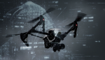
Drones as Weapons
The successful drone attack against Saudi Aramco likely used high-end commercial or low-grade military devices, but earlier attempts were reported with consumer and commercial level drones. Regardless if it is a few big payload devices or a swarm of smaller commercial level drones, serious damage can be inflicted. In the past, Saudi Aramco suffered one of the biggest hacking incidents on record where a crushing attack on their computer infrastructure destroyed massive amounts of data which shut the company down for an extended period.
Unfortunately, this only the beginning. Imagine if the drones and computing attacks happened in coordination. Hackers might manipulate industrial IoT control surfaces such as valve manifolds, petroleum processing equipment, and storage pressurization to prepare for maximum damage. They could then disable safety overrides and fire suppression systems while drones move in to initiate kinetic damage. These facilities are basically big chemical plants with highly flammable contents. Such synchronization could greatly amplify the effects, resulting in a massive impact.
The cybersecurity strategy community predicted such tactics and many more issues across this space, including downing airliners, destroying power grids, terror attacks on crowds in large public gatherings, assassination attempts on political and religious leaders. The list goes on.
The fictitious Slaughterbots video released two years ago highlights some disturbing possibilities along these lines. Much of the core technology capabilities does currently exist for killer drones, although to my knowledge it has not yet been assembled with lethal payloads and coordinated to operate in an AI swarm configuration. It is just a matter of time until some group does take the next step.
Looking back over the last three years, many of us in the cybersecurity world predicted drone attacks. Some paid attention and a few forward-thinking companies started developing countermeasures, but by and large, most of the market ignored the warnings. This lack of interest has opened a window of opportunity for attackers. Although funding has been scarce, it is fortunate that some innovation continued.
On the consumer side, the tools to control errant or malicious drone use has made progress. Many techniques have been explored, from birds of prey (yes birds) plucking drones from the sky, to projectile nets, signal jamming, and navigational electronic interference. Hobbyist drones are easier to counter because of their limited range, but there are some commercial drones that can travel 10+ miles with a payload. The drones that are being used to damage targets in Saudi Arabia, which struck the oil refinery this week, are likely larger low-end military designed units (X-UAV or Qasif types) with much greater range and destructive capacity. Those represent a far different challenge but are now part of the scope that organizations and governments must contend with. More sophisticated detection and eradication systems are beginning to make their way to market in limited numbers.
The Bigger Problem
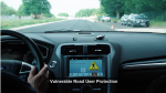
The problem is not limited to drones, but rather the combination of all the technology that is connected. Innovation is pushing digital functionality and enabling new device features for automation, accessibility, and remote operation. As we hand over control to autonomous devices, such as cars, buses, and planes, we then put the safety of drivers, passengers, other vehicles, and pedestrians at risk.
Upgrades to major industrial facilities opens risks of being compromised which could lead to industrial accidents such as chemical spills, fires, and water contamination. With major critical infrastructure elements being automated and accessible remotely, the foundations of our society are put in jeopardy. Electricity, water, sanitation, food distribution, emergency services, healthcare, and communications are at significant risk.
Many targets, beyond industrial and manufacturing, will likely be considered by attackers. Airports, shipping vessels, major sports/entertainment stadiums, political gatherings, government leaders, transportation infrastructure, electrical networks, fresh-water plants, etc. are all potentially at risk from connected technology. Attackers may be able to tamper with or destroy systems, distribute harmful materials, interfere with services, or violate the privacy of citizens. We should expect that violent groups will use whatever tools and techniques necessary to reach across the globe as it suits their needs.
Welcome to a New Era in Human Conflict
A synthesis of digital and physical tools that will be leveraged across the spectrum, from traditional open combat, asymmetric and guerrilla warfare, terrorism and religious extremism, citizen revolts, and low-intensity conflicts such as political protests and suppression.
Cybersecurity is needed, in conjunction with traditional physical security, to manage evolving risks. It is imperative we recognize the global strategic challenges and work together to lay the necessary foundation for strong security defenses and trust in future technology. Only looking at yesterday’s risks or today’s crisis is NOT enough. We must have the vision and courage to look forward and maneuver to manage the risks of attacks in the future.