There were many interesting presentations at ARM TechCon this year besides the keynote addresses by Arm, which were truly stunning for content and production value. One very interesting presentation was the talk given in the afternoon of Wednesday, October 9, 2019, titled, Synopsys Fusion Compiler for Next Generation Arm Hercules Processor Core in Samsung 5nm Technology. The presentation was split into three sections given by Sudhir Koul, Director Engineering SoC Design, Samsung; Leah Schuth, Director, Technical Marketing, Arm; and Dale Lomelino, Sr. Applications Engineer, Synopsys.
Trying to implement a new processor on a new technology node is a substantial challenge. To make that work, a focused collaboration between the teams involved in the process rules, IP design, and EDA tools is mandatory. The first part of the presentations paid much attention to that aspect, the close interaction between the different teams at Samsung, Arm, and Synopsys. If you are going to try to implement this processor on this chip, then you will be receiving support from Samsung and Arm as well. But the support they can provide will have been enhanced, especially if you are using Synopsys tools, by the project discussed in the presentation. So, for the rest of this blog, I will focus on the EDA tools provided by Synopsys, as this is the key variable if you have already chosen the process and core you wish to implement.
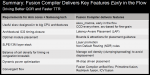
The final portion of the presentation discussed the Synopsys implementation, which revolved around the Synopsys Fusion Design Platform, and its key component, the Fusion Compiler RTL-to-GDSII product. Fusion Compiler is a confluence of leading-edge technologies, previously deployed as standalone solutions, being deployed together atop a single, converged data-model – synthesis, place & route, and sign-off tools all together in a singular product. Synopsys is the EDA company with the richest tradition in providing synthesis technology – it was the technology foundation on which the company was initially built. The fusing of synthesis with P&R and sign-off tools on a single data model with a common interleaved optimization framework is what makes Fusion Compiler special.
Clocks have never traditionally featured in the synthesis space; logic optimization is done assuming ideal clocks with zero skew as a target. Arm-core designs – and many others – rely on clock skew to not only enable the high-performance numbers required in datacenter scenarios, but the very architecture demands it to optimize data timing into-and-out-of memory structures – like cache lookups – as part of the data-paths. By having a single data-model that all engines work off, Fusion Compiler can deploy concurrent-clock-and-data (CCD) optimization – traditionally a backend technology – in the early phases of synthesis to create offset or target skews and thus provide the optimization infrastructure with a better view of what is required during logical/physical implementation. Synopsys refers to this as “CCD Everywhere.” This technique implies that the logic and timing information, including clock skew, can be utilized to optimize the design at many different places within the toolchain. The approach more easily allows the use of “useful skew” when trying to meet timing requirements. But, it can also mean that knowledge of useful skew can allow a datapath to be de-prioritized to improve the performance on some other critical path. These are the types of trade-offs you can imagine inside the Fusion Compiler’s common optimization engines.
I do not want to imply that all the benefits in the Fusion Compiler come from the utilization of CCD technology. In the presentation, Synopsys also discussed other advanced technologies, including latency-aware placement (LAP), layer binning, layer promotion, and non-default routing (NDR) technologies.
NDRs are an especially interesting concept where signal nets can be made wider to lower their resistance, thereby improving timing. It effectively gives the layout tools access to an additional logical layer bin to which timing critical paths can be assigned. This concept sounds simple, but automating this feature is not trivial, and for that reason it is an interesting development.
Overall, I think that designers can take comfort from the efforts described in this presentation for two reasons: (a) if you want to implement the Arm Hercules processor in the Samsung 5LPE process, this project generated much information that these companies can share with you in order for you to implement your project efficiently; and (b) implanting any design in the 5LPE process with Synopsys tools should be easier since this project paved the path. Congratulations to Samsung, Arm, and Synopsys for pulling off this collaborative project.