RVN! 26 Banner revised (800 x 100 px) (600 x 100 px)

Xilinx Moves from Internal Flow to Commercial Flow for IP Integration

Xilinx Moves from Internal Flow to Commercial Flow for IP Integration
by Daniel Payne on 08-25-2020 at 10:00 am

Xilinx IP min

I’ll never forget first learning about Xilinx when they got started back in 1984, because the concept of a Field Programmable Gate Array (FPGA) was so simple and elegant, it was rows and columns of logic gates that a designer could program to perform any logic function, then connect that logic to IO pads to drive other chips on the board. At first their chips were used to gather up all of the glue-logic found on a printed circuit board which was hundreds of logic gates, but today that situation is drastically different because with the new Adaptive Compute Acceleration Platform (ACAP) architecture they have managed to pack 50 billion transistors on a single die with an impressive IP library.

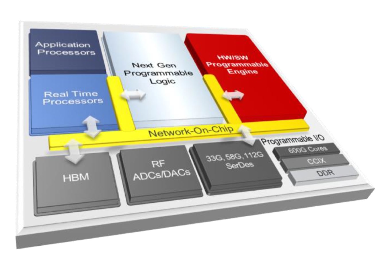
Xilinx has figured out how to offer SoC designers lots of features through IP blocks, and the fastest-growing market segments are loving it: AI, ADAS, IoT, Cloud computing, data center. Designers now have access to a wide range of configurable IP like:

  • Application processors, ARM cores
  • Real time processors
  • High Bandwidth Memory (HBM)
  • RF, ADC, DAC
  • SerDes
  • Programmable IO: CCX, DDR
  • Network-On-Chip
  • Programmable Logic

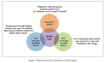
Nitin Navale from Xilinx presented at DAC on the topic, “IP Integration Challenges of Domain-Specific Architectures on Programmable SoC Platforms“, so I watched the 22 minute presentation and summarize the major findings in this blog.

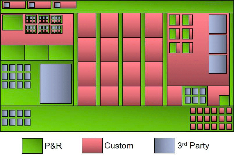
Near the end of an SoC project all of the physical IP needs to be integrated together in a correct manner, quickly and with disk storage efficiency. The top-level for a Xilinx chip is constructed in a hierarchical fashion, but with different layout styles, like:  Custom layout, Place & Route (P&R). In addition, each IP block is either developed internally, or provided by a third party. Data formats for IP blocks can be in GDS II, LEF/DEF or the newer Oasis format.

Here’s a diagram showing how P&R blocks, custom blocks and 3rd party blocks can be assembled in a complex hierarchy to form a Xilinx SoC.

An IP block may contain P&R regions and some Custom, or P&R and some 3rd party, or Custom with P&R blocks, so lots of permutations are possible. It’s important that consistent versions of an IP are maintained across the entire hierarchy, so no mismatching versions can be allowed.

As an IP block has been verified clean and is no longer changing, it gets marked as Golden, so no further revisions are accepted. Having a QA methodology for checking and preserving IP integrity is a requirement, because getting to market with first-pass silicon success is what keeps a company profitable.

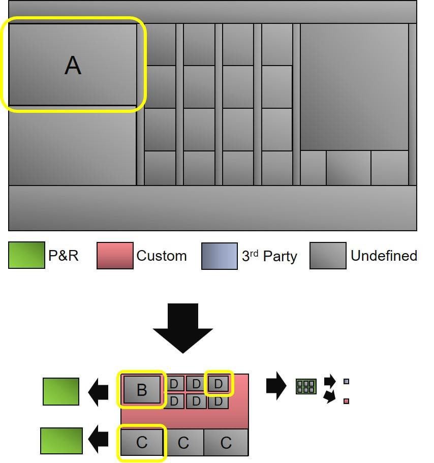
Xilinx formerly used an internal flow for IP integration, but now they prefer using a commercial EDA tool flow. Using the previous hierarchy diagram as a basis, consider how we want to trace the chip hierarchy in order to identify all IP layout data to build a merge list:

  1. Retrieve IC layouts for all top-level blocks
  2. Review each layout for undefined sub-blocks
  3. Recurse on undefined sub-blocks

This diagram shows how we start out at the top-level and identify Block A, recurse into it and find Blocks B, C and D. Recurse into Block D and find the lowest leaf cells.

Custom blocks are defined using OpenAccess, so the integration task is to stream out the GDS II from OA. Most 3rd party designs are stored on Unix as a GDS II file, so integration requires retrieving the Unix path. A P&R block could be saved either as Oasis or GDS II, so a custom script makes that decision.

In step 2 they use another utility to recurse and find any undefined sub-blocks. In the example both Bock B and C are defined as P&R blocks, while Block D is made up of 3rd party  IP.

This methodology continues for all blocks on the Xilinx chip, identifying between 40 and 70 layout files, so finally it’s time to merge the data. The internal CAD tool flow required two steps, creating a very large intermediate GDS II file, then converting that GDS II into the final Oasis file to satisfy the foundry. Problems with the internal tool flow:

  • Slow run times
  • Disk intensive
  • Cannot mark a layout as Golden

The new tool adopted at Xilinx for IP merge integration is called Skipper, and it’s from Empyrean. There were several reasons that Skipper was so attractive:

  • Fastest speed for both GDS II and Oasis viewing
  • Fast IP merging, 5-10X speedup
  • One step method, instead of two
  • Smaller disk space usage
  • Integrated with 3rd party DRC/LVS tools, easy to debug
  • Speedy LVL runtimes

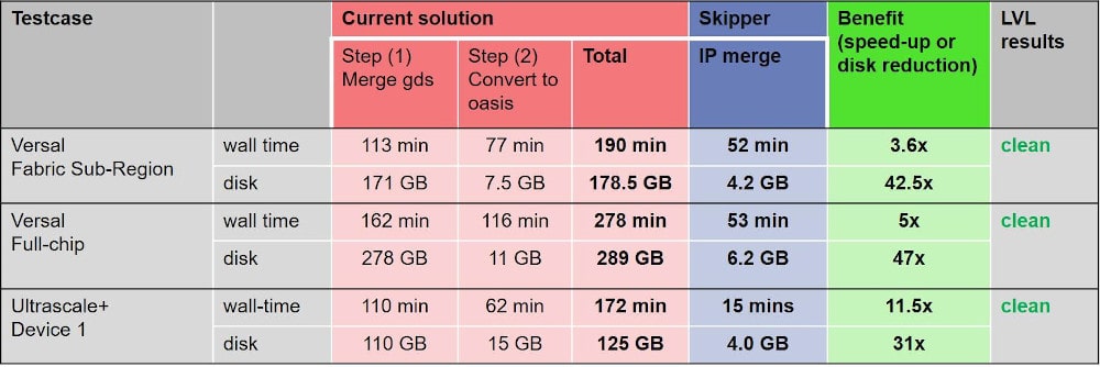
The proof of these improvements is shown in a comparison of both runtime and disk usage on three test cases:

Runtime speed improvements range from 3.6X to 11.5X, while disk usage is quite impressive at 31X to 42.5X smaller when using Skipper.

Summary

A 50 billion transistor programmable SoC from Xilinx is a dazzling achievement because of the sheer engineering challenges, and the CAD team has moved from an internal IP integration methodology to a commercial tool flow using Skipper from Empyrean. Both run time improvements and disk efficiency metrics were quite convincing to make the switch. Watch the entire 22 minute video on YouTube.

Related Blogs


Netlist CDC. Why You Need it and How You do it.

Netlist CDC. Why You Need it and How You do it.
by Bernard Murphy on 08-25-2020 at 6:00 am

netlist cdc min

The most obvious question here is “why do I need netlist CDC?” A lot of what you’re looking for in CDC analysis is really complex behaviors, like handshakes between different clock domains, correct gray coding in synchronizing FIFOs, eliminating quasi-static signals and the like. Deeply functional, system-level intent stuff. How on earth could you deal with that at the netlist level? Not to mention that you’re already battling massive levels of false negatives. Wouldn’t these be a thousand times worse in a netlist design? Well yes, but – synthesis, ECOs, CTS and the like can mess up a lot of details relevant to CDC, during implementation. Which is why you also have to run CDC on netlists. The question then is – how?

Yes, you still have to do RTL-based CDC

First, I don’t believe anyone is claiming you can ignore CDC analysis at RTL and start from scratch on a netlist. RTL CDC is still essential to do all that functional/intent-based analysis, and to build up lists of exceptions and waivers. Because you’re going to need those controls and constraints for your netlist-based CDC. You’re also going to have to be careful with what netlist names you use in those controls. For example, not using names that may disappear in synthesis. The constraints and controls you develop in this RTL-level analysis will then be the starting point for netlist-based CDC.

Design changes in implementation

Second, what does implementation change that requires re-running CDC? Quite a lot. From a big-picture behavior point of view it’s low-level stuff, though still very important to CDC correctness. Some of these spring from optimizations in synthesis, for example design restructuring to optimize timing. Flip-flops move around in paths, causing CDC-correct pre-synthesis logic to become invalid. Some power related capabilities must be inserted in implementation. Some DFT choices are floorplan sensitive (such as MBIST controller sharing), requiring they be updated in implementation. Clock-tree balancing is a very delicate task, continuing to evolve in implementation, not only to optimize skews but also as clock gating plans evolve.

New CDC problems can also arise through ECOs. A functional, timing or power problem discovered late in implementation may force a logic change in the netlist, one reason we need netlist equivalence checking. Unfortunately EQ doesn’t help with CDC. Going all the way back to the RTL to fix a functional problem is too big a hit to the schedule at this late stage. More changes, more need to recheck CDC.

Glitching

Logic gates can glitch when two or more inputs change at the same time. The output briefly flips then flips back again. Not a big deal when the gate is safely cocooned between two levels of registers. But it can be a very big deal if the gate is controlling a clock or an asynchronous reset around a clock (or reset) domain crossing. These hazards can’t always be fixed at RTL. Synthesis can choose how to implement functions like muxes, for example, if you don’t carefully constrain the choice. The default synthesis selections may be glitch prone. You can’t figure this out until after synthesis.

VC SpyGlass for netlist CDC

Synopsys has adapted SpyGlass CDC to be well aligned with these netlists CDC needs. Designers benefit with VC SpyGlass’ ability to support huge designs (1.5 billion+) and a robust Tcl environment to reduce design setup between implementation and verification flows, including the ability to develop their own design query scripts and generation of custom reports. The tool also supports features I’ve mentioned in earlier blogs, such as machine learning root cause analysis (ML RCA) help to generate constraints to reduce noise and hierarchical flow support to improve

You can learn more from this white paper.

Also Read:

The Big Three Weigh in on Emulation Best Practices

Synopsys Presents SAT-Sweeping Enhancements for Logic Synthesis

DAC Panel – Artificial Intelligence Comes to CAD: Where’s the Data?


Semiconductors Not as Bad as Expected!

Semiconductors Not as Bad as Expected!
by Bill Jewell on 08-24-2020 at 4:00 pm

img 5f444eedf131d

In the early stages of the global COVID-19 pandemic, most forecasters expected the semiconductor market to decline in 2020, including our May Semiconductor Intelligence projection of a 6% drop. However, the semiconductor market has shown surprising strength so far this year. WSTS reported the 2Q 2020 semiconductor market was only down 0.9% from 1Q 2020. The top semiconductor companies had mixed results for 2Q20. Nvidia’s acquisition of Mellanox and Infineon’s acquisition of Cypress increased their 2Q20 revenues. These acquisitions are excluded in the comparison of 2Q20 to 1Q20. The total revenues of the twelve companies listed were up 3.9% in 2Q20 from 1Q20. Seven of the twelve companies had revenue declines. The memory companies (Samsung, SK Hynix, Micron and Kioxia) were up 12.7% while the non-memory companies were down 1.4%.

The consolidated 3Q20 guidance of the non-memory companies is 4% revenue growth from 2Q20. However, the guidance is dragged down by Intel’s guidance of -7.7%. Excluding Intel from the non-memory companies, the resulting 3Q20 guidance is 15%.

The major memory suppliers did not provide guidance for 3Q20 revenues, except for Micron Technology. However, they all stated new products in smartphones and videogames are expected to drive revenue growth in the second half of 2020. Apple is expected to introduce its 5G iPhone 12 models in October. Microsoft will release its Xbox Series X gaming system in November. Sony is expected to release its PlayStation 5 gaming system before the end of 2020. In late June, Micron said it expected revenues to increase from 6% to 15% for its quarter ending in late August. However, in a financial conference earlier in August, Micron said the quarter would be “somewhat weaker” than its previous guidance.

IDC in late May and early June of this year forecast double-digit declines in 2020 for both smartphones and PCs. July data on 2Q 2020 shipments showed smartphones were down 16% versus a year ago – in line with IDC’s June forecast of an 11.9% decline in 2020 smartphone shipments. July data on 2Q 2020 PC shipments showed a surprising 11% year-to-year increase driven by increased use of PCs for working and learning from home during the pandemic. IDC will certainly revise its 2020 PC forecast upward from its May forecast of a 15% decline, possibly showing an increase in PC units for the year 2020.

The global recession of 2008 to 2009 was the worst economic downturn since the great depression in the 1920s and 1930s. In 2009, the global GDP declined 1.7% and U.S. GDP declined 2.5%, according to the World Bank. The current global recession will certainly be much worse than 2009. The June economic forecast from the International Monetary Fund (IMF) was a 4.9% decline in global GDP in 2020. The advanced economies will be hit the worst, with an 8% decline. Emerging and developing economies are expected to decline 3%. Ironically, the only major economy expected to show growth in 2020 is China – the original source of the COVID-19 outbreak. The IMF projects global GDP will recover to 5.4% growth in 2021. Looking at the net change in GDP from 2019 to 2021, the advanced economies should see a 3.6% decline while the emerging and developing economies should see a 2.7% increase.

As pessimistic as the IMF economic update was in June, the COVID-19 pandemic has become more severe since. According to Johns Hopkins University, worldwide COVID-19 cases more than doubled from 10.5 million at the end of June (after the IMF report) to 23.4 million as of August 23. U.S. cases also more than doubled during the same time period, 2.6 million to 5.7 million. Recently cases have been increasing in hard-hit countries which seemed to have had COVID-19 under control such as the UK, Spain, France, and Italy.

Against this backdrop, we at Semiconductor Intelligence find it difficult to expect much of an increase in the world semiconductor market in 2020. However, the strength of the PC market and the relatively optimistic 3Q 2020 guidance of several major semiconductor companies indicates the semiconductor market will fare better than the overall economy in 2020. We are forecasting 1% growth in the semiconductor market in 2020 and 8% growth in 2021. Several recent forecasts for 2020 are around 3%. The Cowan LRA Model predicts 5.2% growth in 2020, but this model is based on historical trends and does not account for the current pandemic. For 2021, the Cowan LRA model forecasts 4.4% growth, WSTS expects 6.2%, and Semico Research predicts “low double digit” growth (shown as 10% on the chart).

We are in uncharted territory in 2020 – the worst pandemic in 100 years and the worst economic downturn in 90 years. The relative strength of the semiconductor market compared to the overall economy is largely due to the shifting nature of human interaction. Most countries have placed restrictions on workplaces, schools, and retail outlets. Thus, people increasingly work, learn and shop from home. This increases demand trends for PCs, smartphones, computing infrastructure and communications infrastructure. Even after the COVID-19 pandemic is over, many of these trends will continue – making semiconductors and electronics an even more important part of the global economy.

Also Read:

Semiconductors up in 2020? Not so fast

Is the Worst Over for Semiconductors?

COVID-19 and Semiconductors


Moving to Deeply Scaled Nodes for Power? There is a Better Way

Moving to Deeply Scaled Nodes for Power? There is a Better Way
by Mike Gianfagna on 08-24-2020 at 10:00 am

AGGIOS Definition

Did you know you can save 30% to 60% power without spending a fortune on a process migration? There is a better way than moving to deeply scaled nodes for power. Read on…

Have you heard of AGGIOS? You will. The name stands for AGGregated IO Systems, and a team of ex ARM and Qualcomm engineers are re-inventing power management. I’ll explain what AGGIOS is up to in a moment, but first a bit of backstory is in order to set the stage for why AGGIOS technology is so important.  It’s a story of “three P’s”.

Price

For decades, semiconductor companies rode the Moore’s Law curve and migrated to the next process node every two to three years to get the latest boost in performance and reduction in power and area. Lately, that is slowing down quite a bit with a cycle of five to seven years (or more). The price to migrate is skyrocketing and the power benefits are rapidly diminishing.

Gartner estimates the price tag to design a 7nm SoC to be $270 to over $400 million. This is at least 3x more than the design cost for a 16nm SoC. Costs per chip stay manageable only if end user needs are addressed and the market is large enough to absorb design costs. If you are Apple or Samsung, you have an infrastructure and customer base to accomplish this.

For everyone else these are rare air prices. Gartner estimates that 7nm delivers 65% power reduction over 16nm. A good result, but at a steep price.  For perspective, from 7nm to 5nm the power gain is just 20% – 30%, according to TSMC and Samsung.

Performance

Performance is no longer the leader of the technology adoption curve. For a long time, it was. You could just move to the next process node, increase your clock speed and have a new, competitive product. The flattening of Moore’s and Dennard’s Laws has changed that.

Instead, system design approaches exploit parallelism. Hardware accelerator and multi-core architectures with high-speed communication backbones are leading the way to superior performance. As these technologies significantly stress the power budget, the same need for power reduction exists.

Power

Because of battery life demands, thermal constraints and overall cost to operate data centers, power optimization has become a primary business and technology driver in the semiconductor sector. Even governments are involved with power reduction mandates. All roads lead to reduced power consumption.

A lot of power reduction strategies focus on hardware and process. I’ve touched on process improvements and the associated price tag. Hardware techniques such as clock gating or voltage and frequency scaling can successfully reduce power consumption when closely aligned with software execution. There is an “elephant in the room” problem with all this, however. These methods can deliver good power reduction, but, as with other approaches, it takes a lot of in-house engineering effort, talent and a company-wide vertically integrated hardware/software infrastructure to make it effective. Again, Apple or Samsung has it. For everyone else, it is a challenge.

Recap

Effective power management is something everyone needs but only a few can afford. Moving to the next process node is prohibitively expensive and the resultant power reduction is going down in advanced nodes. Performance improvements are being driven by architectural innovations that further stress the power budget. Hardware level approaches can reduce power, but the reductions take a lot of skill, effort and costly infrastructure. If you are moving to deeply scaled nodes for power there is a better way.

A Revolutionary Software-Based Approach to Power Management

A basic truth is that SoCs consume power when they run software. Hardware alone has a hard time understanding the dynamic behavior of the application and system software and its impact on power. What would happen if we enable software to directly optimize every milliwatt? AGGIOS saw the opportunity this presented early-on and developed a patented Software Defined Energy Management system. Their technology delivers fine-grained control of hardware power consumption to the software developer and provides fast and accurate feedback on the impact of software optimizations.

Typical power savings range from 30% to 60% with AGGIOS. So, you can achieve the same or better power reduction associated with expensive process migration and extensive engineering effort without hardware modifications or process migration. At last, what used to be an expensive and labor-intensive but valuable portion of power management is now available to all, not just the special few.  AGGIOS products act exclusively through automated system software and firmware optimization enabling longer lasting, cooler and smaller electronic devices delivered on schedule with much lower cost. Their approach can be applied to any SoC or FPGA architecture.

What would you do with all that power savings? You can read about some real case studies in a white paper from AGGIOS. They document actual results on a series of Xilinx Zynq UltraScale+ MPSoC applications using Xilinx Targeted Reference Designs (TRDs) and other reference applications. The applications include video streaming, video deep learning, ECC processing, memory throughput and two software-defined radios. Their white paper provides a lot of detail on the hardware and software architecture of the applications, how AGGIOS software is applied to the design and the detailed results they achieved.

Speaking of results, the actual power savings reported range from 35% to an eye-popping 86%. Recall that a difficult and expensive move from 16nm to 7nm delivers 65% power savings. The AGGIOS approach is even more effective at deeply scaled nodes as it can account for and even exploit the high variability of these processes to reduce energy consumption or increase performance.

If a new, cost-efficient and highly effective power management strategy sounds appealing, you need to download this white paper. It just may change the direction of your next project, especially if advanced technology migration is being considered or if you’re concerned that gains just won’t be enough. There is a better way than moving to deeply scaled nodes for power. You can download the white paper, titled AGGIOS Seedlings Power Reference Designs: Xilinx UltraScale+ here. 


High-throughput Workloads Get a Boost from Altair

High-throughput Workloads Get a Boost from Altair
by Daniel Nenni on 08-24-2020 at 6:00 am

Altair PBS Professional 2020 1

Altair PBS Professional™ is the trusted leader in high-performance computing workload management. It efficiently schedules HPC workloads across all forms of computing infrastructure, and it scales easily to support systems of any size — from clusters to the largest supercomputers.

Scheduling for high-throughput workloads just got easier. With the release of Altair® PBS Professional® 2020 we’ve expanded our industry-leading HPC workload manager with brand new capabilities, including hierarchical scheduling that can handle the biggest volumes of small, high-throughput jobs.

PBS Professional 2020

The new hierarchical scheduler built into PBS Professional offloads the base scheduler to enable greater throughput and better license and resource utilization. Batches of short jobs are presented as one longer job while maintaining full visibility into each individual job.

In addition to delivering a single scheduler for all types of workloads, PBS Professional has more new features including:

  • Cloud bursting and dynamic extension with a built-in GUI
  • Forecasting and simulation
  • Allocation and budget management
  • Security, performance, and administrative and usability updates

And PBS Pro users still get all the tools they already rely on for workload orchestration and optimization.

Altair HPC Virtual Summit

Learn about solutions for high-throughput scheduling and more at the Altair HPC Virtual Summit September 9 and 10. We’ve packed two half-days with topics in two tracks including semiconductor design acceleration and HPC and IT optimization, kicking off with PBS Professional User Group sessions in two time zones.

Virtually network with Altair experts, partners, customers, and industry peers to learn about the leading-edge computing solutions that keep innovation moving forward with cost savings and enhanced efficiency. Featured sessions include:

  • Keynote speaker Michael Heroux of the Exascale Computing Project
  • Cloud roundtable: “Is Cloud Officially Inevitable?” featuring participants from Google Cloud, Microsoft Azure, and Oracle
  • Live Q&A with the Altair development team and technical experts

Our track for semiconductor IT pros and engineering experts includes sessions on how to drive efficiency at every step of the design process. Take chip design to the cloud with Rapid Scaling solutions that bring cloud costs closer than ever to real demand, save serious money with license-first scheduling tools, and meet the design flow mapping tools VLSI engineers at leading semiconductor organizations user to get new technology to market first.

Register today to save your spot

About Altair (Nasdaq: ALTR)
Altair is a global technology company that provides software and cloud solutions in the areas of product development, high performance computing (HPC) and data analytics. Altair enables organizations across broad industry segments to compete more effectively in a connected world while creating a more sustainable future. To learn more, please visit www.altair.com.

Also Read

Interview with Altair CTO Sam Mahalingam

Six Essential Steps For Optimizing EDA Productivity

Latest Updates to Altair Accelerator, the Industry’s Fastest Enterprise Job Scheduler


PCI Express in Depth – Physical Layer

PCI Express in Depth – Physical Layer
by Luigi Filho on 08-23-2020 at 10:00 am

PCI Express in Depth Physical Layer

In the last article, I wrote about the PCIe basic concepts. This article will reach the physical layer of the PCIe standard.

The lowest PCI Express architectural layer is the Physical Layer. This layer is responsible for actually sending and receiving all the data to be sent across the PCI Express link. The Physical Layer interacts with its Data Link Layer and the physical PCI Express link.

This layer contains all the circuitry for the interface operation: input and output buffers, parallel-to-serial and serial-to-parallel converters, PLL(s) and impedance matching circuitry. It also contains some logic functions needed for interface initialization and maintenance.

In the physical layer let’s subdivide in two sub-blocks: Logical and Electrical sub-block

Logical Sub-Block

The logical sub-block is the key decision maker for the Physical Layer. The logical sub-block has separate transmit and receive paths, referred to hereafter as the transmit unit and receive unit. Both units are capable of operating independently of one another.

The primary function of the transmit unit is to prepare data link packets received from the Data Link Layer for transmission. This process involves three primary stages: data scrambling, 8-bit/10-bit encoding, and packet framing. The receive unit functions similarly to the transmit unit, but in reverse. The receive unit takes the deserialized physical packet taken off the wire by the electrical sub-block, removes the framing, decodes it, and finally descrambles it.

The figure below illustrate this:

Remember that you need to consider each lane of the PCIe.

Some sub topics in the electrical sub-block:

  • Data Scrambling – PCI Express employs a technique called data scrambling to reduce the possibility of electrical resonances on the link. PCI Express specification defines a scrambling/descrambling algorithm that is implemented using a linear feedback shift register. PCI Express accomplishes scrambling or descrambling by performing a serial XOR operation to the data with the seed output of a Linear Feedback Shift Register (LFSR) that is synchronized between PCI Express devices
  • 8-Bit/10-Bit Encoding – The primary purpose of 8-bit/10-bit encoding is to embed a clock signal into the data stream. By embedding a clock into the data, this encoding scheme renders external clock signals unnecessary.
  • Packet Framing – In order to let the receiving device know where one packet starts and ends, there are identifying 10-bit special symbols that are added and appended to a previously 8-bit/10-bit encoded data packet

Electrical Sub-Block

As the logical sub-block of the Physical Layer fulfils the role as the key decision maker, the electrical sub-block functions as the delivery mechanism for the physical architecture.

The electrical sub-block contains transmit and receive buffers that transform the data into electrical signals that can be transmitted across the link.

The electrical sub-block may also contain the PLL circuitry, which provides internal clocks for the device.

Some sub topics in the electrical sub-block:

  • Serial/Parallel Conversion – The transmit buffer in the electrical sub-block takes the encoded/packetized data from the logical sub-block and converts it into serial format. Once the data has been serialized it is then routed to an associated lane for transmission across the link. On the receive side the receivers deserialize the data and feed it back to the logical sub-block for further processing.
  • Clock Extraction – In addition to the parallel-to-serial conversion described above, the receive buffer in the electrical sub-block is responsible for recovering the link clock that has been embedded in the data.
  • Lane-to-Lane De-Skew – The receive buffer in the electrical sub-block de-skews data from the various lanes of the link prior to assembling the serial data into a parallel data packet. This is necessary to compensate for the allowable 20 nanoseconds of lane-to-lane skew.
  • Differential Signaling – PCI Express transmit and receive buffers are designed to convert the logical data symbols into a differential signal.
  • Phase Locked Loop (PLL) Circuit – A clock derived from a PLL circuit may provide the internal clocking to the PCI Express device. Each PCI Express device is given a 100 mega-hertz differential pair clock. This clock can be fed into a PLL circuit, which multiplies it by 25 to achieve the 2.5 gigahertz
  • AC Coupling – PCI Express uses AC coupling on the transmit side of the differential pair to eliminate the DC Common Mode element. That makes the buffer design process for PCI Express becomes much simpler
  • De-Emphasis – PCI Express utilizes a concept referred to as de-emphasis to reduce the effects of inter-symbol interference.

As always, leave a comment if you want me to get into more details.


PCI Express in Depth

PCI Express in Depth
by Luigi Filho on 08-23-2020 at 8:00 am

PCI Express in Depth

This is another post that was requested by a user, and as always i’ll do my best to put in a few articles the basic information that you’ll need to understand how it works at depth level.

PCI Express (or PCIe) is a high-speed serial computer expansion bus designed to replace the older PCI, PCI-X and AGP standards.

The first principle you need understand is the LANES, a lane is composed of two differential signaling pairs, with one pair for receiving data and the other for transmitting. Thus, each lane is composed of four wires or signal traces. Conceptually, each lane is used as a full-duplex byte stream, transporting data packets in eight-bit “byte” format simultaneously in both directions between endpoints of a link.

The connection between two PCIe devices is referred to as a link, physical PCIe links may contain from 1 to 16 lanes, more precisely 1, 4, 8 or 16 lanes. Lane counts are written with an “x” prefix (for example, “x8” represents an eight-lane card or slot), with x16 being the largest size in common use. Lane sizes are also referred to via the terms “width” or “by” e.g., an eight-lane slot could be referred to as a “by 8” or as “8 lanes wide.”

Others concepts include:

  • PCIe elements types:
  1. Root Complex – Is the head or root of the connection.
  2. PCI Express-PCI bridge – As the name says has one PCI Express port and one or multiple PCI/PCI-X bus interfaces.
  3. Endpoint – is a device that can request/complete PCI Express transactions for itself
  4. Switch – are used to fan out a PCI Express hierarchy.
  • PCIe Transactions Types:
  1. Memory Transaction – Transactions targeting the memory space transfer data to or from a memory-mapped location
  2. I/O Transactions – Transactions targeting the I/O space transfer data to or from an I/O-mapped location
  3. Configuration Transactions – Transactions targeting the configuration space are used for device configuration and setup
  4. Message Transactions – PCI Express adds a new transaction type to communicate a variety of miscellaneous messages between PCI Express devices

The architecture is show in the figure below:

The next three articles will be about theses three layers: Physical Layer, Data Link Layer and Transaction Layer.

As always, leave a comment, just tell me which protocol or standard you want to know more about it.


Fully Self-Aligned 6-Track and 7-Track Cell Process Integration

Fully Self-Aligned 6-Track and 7-Track Cell Process Integration
by Fred Chen on 08-23-2020 at 6:00 am

Fully Self Aligned 6 Track and 7 Track Cell Process Integration

For the 10nm – 5nm nodes, the leading-edge foundries are designing cells which utilize 6 or 7 metal tracks, entailing a wide metal line for every 4 or 5 minimum width lines, respectively (Figure 1).

Figure 1. Left: a 7-track cell. Right: a 6-track cell.

This is a fundamental vulnerability for lithography, as defocus can change the spacing between lines [1], leading to “pitch walking.” This happens when the first and highest orders go out of phase with each other, leading to one diminishing relative to the other. EUV makes things worse by introducing asymmetry between opposite sides of the pupil [2], leading to feature position shift. To get around this, self-aligned patterning is the default alternative. This also offers an exciting opportunity for both 6- and 7-track cells to be produced at the same time on the same chip.

7-track cell process

Targeting a 14-18 nm minimum half-pitch, we expect to use self-aligned quadruple patterning (SAQP) [1]. However, the core features which guide the SAQP consist of unequally sized lines. Specifically, a larger core feature is surrounded by a pair of smaller core features. When patterned lithographically, this also encounters defocus-induced pitch walking. So, it is also preferred to use self-aligned patterning for the core features as well. Self-aligned triple patterning (SATP) [3] naturally can provide the larger feature surrounded by a pair of smaller features. Since the starting pattern is now a single size line/space pattern, there is no threat of pitch walking from defocus. Figure 2 illustrates the self-aligned spacer patterning stages of the process flow for producing the 7-track cell comprising 5 narrow lines surrounded by two wider lines. SATP followed by SAQP (2 x SADP) constitutes self-aligned duodecuple (12x) patterning (SADDP).

Figure 2. Self-aligned spacer patterning stages of the 7-track cell SADDP fabrication process flow. The fourth row indicates the core features for the SAQP stage, consisting of two SADP stages. For self-aligned cutting or blocking purposes, the finally patterned lines are assigned a red or blue color, depending on whether they are on the final spacer interior or exterior, respectively.

6-track cell process

SATP can also produce the SAQP core features for the 6-track cell process (Figure 3) for the same design rules. The main difference is that the SATP starting pitch is 22 times the minimum linewidth or half-pitch instead of 26 times in the 7-track case. With only a ~15% pitch difference, both cases can be patterned using SATP at the same time.

Figure 3. Self-aligned spacer patterning stages of the 6-track cell SADDP fabrication process flow. As in Figure 2, the fourth row indicates the core features for the SAQP stage, consisting of two SADP stages. For self-aligned cutting or blocking purposes, the finally patterned lines are assigned a red or blue color, depending on whether they are on the final spacer interior or exterior, respectively.

Note that the SAQP core features are different from the arrangement that was presented in [4], since it does not use lithographic patterning but SATP. The advantage is that self-aligned line cutting is more effective.

Self-aligned line cutting or blocking

For both the 6-track and 7-track cases presented here, alternate lines, whether wider or narrower, can be assigned to one of two selectively etchable groups (indicated by the red or blue color), depending on whether the location is on the interior or the exterior of the spacers. This is advantageous for patterning line breaks, or cuts (blocks); neighboring lines will not be damaged by cut (block) placement error from overlay. The 6-track cell here maintains this advantage over that shown in [4], where some pairs of adjacent lines from the spacer interiors may still be simultaneously etched.

Pitch walking revisited

The SADDP sequence is essentially four successive SADP stages. Pitch walking will be determined mainly by the spacer deposition thickness control. In the best case, it can be a few to several percent [5,6]. If the spacer exterior is uncovered, it is also subject to etch thinning, which can also lead to pitch walking. This can be addressed by covering the exterior with another deposited layer, against which the spacer etch is selective [7].

Conclusion

The SADDP scheme is an extremely attractive and powerful approach for patterning 6-track and 7-track standard cells for the leading-edge technology nodes. It is currently the only presented approach where the track lithography is free from pitch walking and self-aligned cutting is also conveniently supported.

References

[1] https://www.linkedin.com/pulse/application-specific-lithography-5nm-6-track-cell-frederick-chen

[2] J. Finders et al., Proc. SPIE 9776, 97761P (2016).

[3] US Patent 7807575, assigned to Micron, filed Nov. 29, 2006.

[4] J. U. Lee et al., Proc. SPIE 10962, 109620N (2019).

[5] https://applied-multilayers.com/wp-content/uploads/2017/05/PECVD-DLC.pdf

[6] https://www.researchgate.net/publication/229964576_Film_Uniformity_in_Atomic_Layer_Deposition

[7] US Patent 7732341, assigned to Samsung, filed Mar. 23, 2007.

Related Lithography Posts


HCL Webinar Series – HCL Compass Delivers Defect Tracking and More

HCL Webinar Series – HCL Compass Delivers Defect Tracking and More
by Mike Gianfagna on 08-21-2020 at 10:00 am

Screen Shot 2020 08 02 at 9.37.53 PM

Similar to my last post on the HCL DevOps webinar series, I will cover their presentation of HCL Compass in a webinar that was recorded on July 29 about how HCL Compass delivers defect tracking and more.

This webinar was presented by Steve Boone, head of product management at HCL Software DevOps, Howie Bernstein, product manager for HCL Compass and HCL VersionVault and Leah Nassar, technical lead for HCL Compass.

As before, Steve began by providing on overview of the DevOps portfolio from HCL Software.  This portfolio was launched on June 16, 2020, so these are new capabilities. Steve stressed that all capabilities can be managed on the cloud or on prem, or whatever combination makes sense for your organization. That level of flexibility is refreshing.

Similar to the previous webinar, Howie and Leah discussed the product in an informal style, with a new addition. More on that in a moment. The current Compass product has been on the market for 23 years, starting as ClearQuest from Rational Software.

Howie explained that the product began as a flexible and customizable issue and defect management tool. He went on to explain that HCL Compass delivers defect tracking and more. This includes  lifecycle management  and the ability to customize that capability without coding for a particular organization’s needs. If you’re wondering how far this can go, Howie reported that a North American government is using the tool to manage their Social Security claims process. Now that’s a departure from SoC development.

Howie described a sophisticated customization process for the product that includes a GUI to describe workflow in great detail and a web-based interface to deploy and manage the resultant application. Very flexible with no coding required. The power of the tool became clear as the discussion continued. You’ll need to watch the webinar to get the full effect.

What followed was a unique online demo of HCL Compass presented by Leah. She went through an interactive creation of a defect tracking application. This included the definition of defects. attributes and assignment to employees. Leah went on to show how to deploy the tool in production and track the status and resolution of defects. Methods to communicate between users was also explained and demonstrated. The capability is quite flexible. She explained how to use the simple, out-of-the-box capability (good for small organizations) and how to customize communication with a lot of control if you’re part of a large organization.

What followed was the development of complete defect tracking tool, built in real-time as you watched. There was interesting discussion between Howie and Leah as Howie requested Leah to add new capabilities. Leah was able to do that easily – Howie couldn’t “stump” her. Leah’s command of the product and its application scenarios was both impressive and built confidence in the tool.

As the end of the webinar approached, Steve provided an honest, “from the heart” view of what remote development looks and feels like in the current environment. There were some great observations offered about how tools like HCL Compass can change the game in this “new normal”. To hear more, you’ll need to watch the webinar.

You can learn more about Compass on the HCL website Compass page. The short description provided there is:

Low-Code/No-Code change management software for enterprise level scaling, process customization, and control to accelerate project delivery and increase developer productivity.

And finally, here is where you can watch the webinar on HCL Compass – I highly recommend it.


ARC Processor Virtual Summit!

ARC Processor Virtual Summit!
by Daniel Nenni on 08-21-2020 at 6:00 am

ARC Processor Virtual Summit 2020

The ARC Processor has a rich history. Originally named the Argonaut RISC Processor, it was designed for the Nintendo Game Systems in the 1990s. Argonaut Technologies Limited later became ARC International. My first intimate exposure to ARC was in 2009 when Virage Logic acquired ARC. A year later Virage was acquired by Synopsys and the rest as they say is history.

There was a lot of speculation at the time whether Synopsys would invest in ARC or let it ride off into the IP sunset. Today I can tell you without a doubt that Synopsys has heavily invested in the ARC processor making it a leading configurable processor core for embedded products around the world, absolutely.

Which brings us to the upcoming ARC Processor Virtual Summit. Virtual events are still evolving but in my experience Synopsys does it right so you are not going to want to miss this one.  The topics include: Automotive Security, Safety and Reliability, Artificial Intelligence, Machine Learning, High-Performance, Embedded IoT. Here are some of the presentation abstracts but check out the full agenda to see descriptions of all 18 sessions (they had me at Porsche).

Join us for the ARC Processor Virtual Summit to hear our experts, users and ecosystem partners discuss the most recent trends and product developments in ARC-based processor solutions.  This multi-day event will provide you with in-depth information from industry leaders on the latest processor IP solutions.

Whether you are a developer of chips, systems or software, the ARC Processor Virtual Summit will give you practical information to help you create more differentiated products in the shortest amount of time.

Frank McCleary
Associate Partner, Porsche Consulting, Inc.
Accelerating Development of Functionally Safe Automotive Systems
The increasingly complex electronics hardware and software architectures of next-generation autonomous, connected, and electric vehicles represent new and daunting challenges for automotive engineering teams. This keynote by Porsche Consulting, Inc. will discuss how automotive development organizations can accelerate silicon chip design with automotive-grade IP, speed software development with virtual prototypes, and address functionality safety and reliability throughout the development lifecycle.

Jeff Bier
Founder, Edge AI & Vision Alliance / President, BDTI
Key Trends in the Deployment of Edge AI and Computer Vision
With edge AI and computer vision technologies advancing rapidly, it can be difficult to see the big picture. This keynote will describe the four most important edge AI and vision trends that are influencing the future of the industry: deep learning; streamlining edge development; fast, cheap, energy-efficient processors; and new sensors. Bier will highlight key implications for technology suppliers, solution developers and end-users. In addition, he will illustrate each of these trends with technology and application examples.

A Single SoC Architecture for Managing the Varying Performance Requirements of Multiple Automotive Applications
Presenter: Konrad Walluszik, Concept Engineer, Infineon
A key trend in the automotive industry is to develop safer, smarter and more eco-friendly cars. Accomplishing this requires innovative semiconductor products that can address a variety of automotive use cases such as domain controllers, e-mobility and advanced driver assistance systems (ADAS).

This presentation describes the challenges of addressing varying performance workloads with a homogenous SoC family targeting different automotive application domains. Leveraging the capabilities of a highly-configurable ARC Vector DSP solution allows scalable SIMD performance, supplemented by a uniform ecosystem to address the family concept. Based on application examples the presentation will show how corresponding challenges are solved by optimized ARC processors.

Safe & Secure SoC Architectures for Autonomous Vehicles
Presenter: Fergus Casey, R&D Director, Synopsys
Let’s face it: People are bad drivers. The Driver is the biggest uncertainty factor in cars, and computer vision is helping to eliminate human error and make the roads safer. Autonomous vehicles are expected to save almost 300K lives each decade in the United States, but after 4-5 decades of autonomous car proof of concepts and years of development, driverless cares still seem a long way off. This presentation will describe the challenges that SoC designers and OEMs face when developing self-driving vehicles, from understanding how a pedestrian looks to software/silicon, to understanding an entire scene. It will then describe the key milestones that the industry, and each chip design, must reach on the road to autonomous driving, and how to know when you’ve reached them.

How to Execute AUTOSAR Classic Projects from a Tooling Perspective on the ARC Functional Safety Processor IP
Presenter: Chris Thibeault, Head of Partner Management – Americas, Elektrobit
Electronic control units (ECUs) empower vehicle functionality, and tooling is an essential aspect of AUTomotive Open System ARchitecture (AUTOSAR) Classic for ECU development.  In this presentation, attendees will learn how the AUTOSAR Standard has evolved. In addition, best practices to set up a typical configuration and integration workflow, including tooling aspects of the AUTOSAR methodology using Elektrobit’s solution for AUTOSAR Classic, as well as configuring AUTOSAR basic software modules and translating the code running on Synopsys’ Functional Safety Processor IP will be covered.

SoC Level Safety Management, A Software View
Speaker: Anatoly Savchenkov, Software Engineering Manager, Synopsys
Increasing complexity of automotive ICs consisting of multiple heterogeneous processors and accelerators, I/O interfaces and custom hardware blocks raises unprecedented challenges for safety architects. Safety management tasks including safe boot, periodic safety testing and handling of runtime safety escalations traditionally are done in hardware making them expensive and not easily reusable in multiple designs. This presentation describes how Synopsys safety hardware architectures are enabled by ARC embedded safety software to deliver increased usability, extensibility, and robustness for SoC level safety management tasks.

Implement ASIL D-Compliant ARC Processor IP Using Synopsys’ Native Automotive Design Solution
Speaker: Shiv Chonnad, Sr. Quality Engineer, Synopsys
Next-generation autonomous driving and advanced driver-assistance systems (ADAS) applications require complex safety-critical electronic components. The SoC designs used in these electronics should adhere to the ISO 26262 functional safety (FuSa) standard to achieve the highest automotive safety integrity level (ASIL). Synopsys offers the broadest portfolio of silicon-proven automotive-grade IP, which is ISO 26262 certified up to ASIL D, for use when developing safety-critical SoCs. Synopsys’ new native automotive RTL-to-GDSII solution, driven by FuSa intent, enables designers to efficiently implement and verify FuSa mechanisms in order to achieve target ASIL with improved quality-of-results and ease-of-use. The Solutions Group IP team has successfully leveraged the native automotive RTL-to-GDSII solution. This presentation will describe the ASIL D-compliant ARC processor IP and the new native RTL-to-GDSII solution, the resulting implementation flow with an ARC HS46 dual-core lock-step (DCLS) processor, and benefits for the SoC designer.

Addressing the Challenges of RADAR, LiDAR & Vision Sensor Fusion for Next-Generation Automotive ADAS Systems
Speaker: Pieter van der Wolf, Principal R&D Engineer, Synopsys
Automotive ADAS systems use multiple sensing technologies, RADAR, LiDAR and Imaging to create a 360 degree view of surroundings. Each different sensing technology has its own advantages to environmental conditions. Complexity is increasing in ADAS systems, while demanding a reduction in component cost. This presentation will go through the computation capabilities of various Synopsys ARC processors as well as discuss the use of cross computation and sensor fusion functionality to improve the quality of sensor detected object data in automotive ADAS systems.

REGISTER HERE AND JOIN US FOR THE ARC PROCESSOR VIRTUAL SUMMIT

Also Read:

Synopsys Webinar: A Comprehensive Overview of High-Speed Data Center Communications

Accelerating High-Performance Computing SoC Designs with Synopsys IP

Quantifying the Benefits of AI in Edge Computing