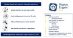
You are currently viewing SemiWiki as a guest which gives you limited access to the site. To view blog comments and experience other SemiWiki features you must be a registered member. Registration is fast, simple, and absolutely free so please, join our community today!
Semiconductor technology advances have a way of rewriting the rule book. As process geometries shrink, subtle effects graduate to mainstream problems. Performance curves can become inverted. And no matter what else occurs, low power demands are constantly reducing voltage and design margins along with it. Sometimes these problems can be solved by just being more careful, and sometimes they require a new way of approaching the problem altogether.
I had an opportunity to explore the latter case recently. I spent some time with Brandon Bautz, senior product management group director and Hitendra Divecha, product management director in the Digital & Signoff Group at Cadence. Both of these gentlemen have been working on advanced chip designs for more than 20 years, so I was in good hands.
We discussed the new Cadence Tempus™ Power Integrity Solution, or Tempus PI, for short. Why is this so interesting and important? Winding back the clock a bit, Hitendra began by explaining that customers had reported max frequency failures in advanced node silicon. The problem manifested with up to 10 percent performance degradation. This translates to hundreds of megahertz out of spec, so it gets attention. Thanks to low power/low voltage operation requirements, you can’t margin your way out of this problem. There just isn’t enough margin. So, what’s causing these failures, and what’s the fix?
The root cause appeared to be related to localized IR drop, but there is a twist. As the process moved from 28nm to 7nm, conductor resistance through the power grids has increased by 10X. This means the traditional method of inserting decoupling capacitors to alleviate localized IR drop is no longer as effective. Also, the change in cell delay vs. voltage becomes much steeper at low voltages in advanced processes. This means a small IR drop will create a large change in timing. These effects are summarized in the diagram below.
Since timing and IR drop have a co-dependent relationship, the designer needs an automated method to simulate the design such that both timing and IR drop problems are simultaneously considered. A user-defined vector approach is difficult as enough vectors to find the problem will create huge runtimes. Random vector approaches create too many combinations as well. It’s a bit of “needle in a haystack” problem. Aggressor and victim nets also need to be considered if there is simultaneous switching and coupling.
We then talked about the architecture of the Cadence signoff tools, specifically how Tempus™ Timing Signoff Solution and Voltus™ IC Power Integrity Solution have been built on a common database and runtime model from the start. By adding additional analysis capabilities to the mix, including machine learning techniques for vectorless stimulus, Tempus PI delivers IR drop-aware STA signoff—that is, voltage analysis that is timing-aware, and timing analysis that is voltage-aware. Using resistance, power, IR-drop and timing data, Tempus PI’s algorithm can identify voltage sensitive paths and potential aggressors. The result is a well-thought-out approach as to what timing paths and aggressors need to be carefully analyzed—not just random activity—solving the “needle in a haystack” problem.
Using the Innovus™ implementation System, timing and IR-drop problems can even be fixed with the ECO flow. As we continued our discussion it became clear the integrated nature of the Cadence tool suite was paying big dividends when it comes to addressing new problems that require simultaneous views to sort out. The figure below summarizes the complete flow.
The Cadence folks shared some results for the ECO flow on a CPU core design:
Before: 1,334 IR-drop victims, 110.5 mV peak IR-drop voltage
After: 87 IR-drop victims, 81.9 mV peak IR-drop voltage
93% fewer victims, 26% less peak IR with no setup/hold degradation. Impressive.
We concluded our discussion with a few customer case studies. I’ll cite two here, and they’re both 7nm designs.
Case 1: An extensive set of activity vectors was used by the customer to perform IR drop analysis. Of the top ten IR drop paths, four were confirmed as top risks with Tempus PI, but Tempus PI found six other top paths that were missed by the vector approach.
Case 2: Tempus PI identified 2,092 critical paths that would have been missed by the customer’s traditional derating method.
At this point, I’m a believer. By making IR drop analysis timing-aware, the new challenges of advanced technology can indeed be tamed. If you’re seeing these kinds of challenges, you should talk to Cadence.
This has got to be one of the most interesting and disruptive EDA acquisitions I have seen in some time. Another one that comes to mind is Siemens acquiring Mentor Graphics. We have been covering EDA PLM companies since the start of SemiWiki and have worked with most of them. If I had to keep score I would say it’s about even but it was just a matter of time before one of them busted loose, absolutely.
The press release is included but first let’s take a look at the Perforce company history based on their Wikipedia page to better understand what this acquisition really means and we can do a Q&A in the comments section.
Perforce Software was founded in 1995 in Alameda, California by Christopher Seiwald, a software developer and computer science graduate from UC Berkeley. Its first product was also called Perforce, and was a version control system allowing companies to collaborate on large software projects by keeping track of changes to both the source code and binary files.
In June 2013, the company released Helix Swarm, a tool for developers working in different geographical areas to collaborate on code review.
In June 2014, the company released a version of its Perforce versioning engine, by then known as P4D, which supported concurrency, the ability of a program to run multiple parts concurrently.
In March 2015, the company renamed its product as Perforce Helix. In October, the company collaborated with GitLab to release GitSwarm, a software tool that combined git distributed workflow for developers with Perforce’s single code repository.
In February 2016, Seiwald sold the company to investment group Summit Partners. The company headquarters was relocated to Minneapolis. In November, Perforce announced the acquisition of Seapine Software, a provider of application lifecycle management (ALM) tools. Seapine’s TestTrack ALM software was rebranded as Helix ALM.
In September 2017, the company acquired Uppsala, Sweden-based Hansoft, a developer of Agile planning software. Also in September, Perforce announced it had acquired Finnish repository management services company Deveo. Deveo’s products were merged into Perforce’s Helix TeamHub, its first solo venture for Git-based development teams.
In January 2018, Summit Partners sold Perforce to private equity firm Clearlake Capital. In May, Perforce acquired UK-based Programming Research (PRQA), a static code analysis firm.
In December 2018, Perforce announced the acquisition of Perfecto, a market leader in cloud-based automated mobile and web application test software solutions.
In January 2019, Perforce announced the acquisition of Rogue Wave Software, a software company with a focus on development tools for high-performance computing.
In April 2019, private equity firm Francisco Partners acquired 50% of Perforce, becoming an equal partner with Clearlake Capital.
In July of 2020, Perforce announced the acquisition of San Francisco based Methodics.
Perforce Continues to Grow Platform Already Used by Top Semiconductor Companies
MINNEAPOLIS, SAN FRANCISCO, and SANTA MONICA, July 20, 2020 – Perforce Software, Inc. (“Perforce”), a provider of solutions to enterprise teams requiring productivity, visibility, and scale along the development lifecycle, backed by Clearlake Capital Group, L.P. (together with its affiliates, “Clearlake”) and Francisco Partners, today announced it has acquired Methodics Inc. (“Methodics”), a leading provider of intellectual property lifecycle management and traceability solutions for the enterprise. The addition of Methodics further distinguishes Perforce in the DevOps market as a solution provider uniquely addressing the needs of some of the largest technology teams in the world facing extreme scale, time to market, and quality imperatives. Terms were not disclosed.
Perforce and Methodics previously had a strategic partnership in place, providing a fully integrated solution to manage IP from design all the way through production and reuse in the semiconductor industry. Many of the world’s top semiconductor companies already leverage Perforce and Methodics for electronic design and data management.
“The semiconductor and embedded software design markets continue to expand, especially as they serve growing AI, automotive, cloud, and IoT markets,” said Mark Ties, Perforce CEO. “Together with Methodics, Perforce will enable these markets to drive faster time to market, higher quality, greater operational efficiency, and increased security and compliance at scale. We are also excited about the opportunity to extend this joint solution into gaming, automotive, and other industries.”
“The importance of collaboration between multisite and multi-geographic design teams continues to intensify. Methodics solutions enable critical collaboration while assuring full traceability and reuse of important design assets and their associated metadata,” said Simon Butler, Methodics CEO. “We are excited to join the Perforce team, and we are confident that this acquisition will enable us to meet the needs of the semiconductor and embedded systems markets, as well as gaming, automotive, and beyond.”
“Maxlinear has been using Perforce Helix and Methodics IP life cycle management solutions for the past few years to increase our productivity and introduce a IP reuse methodology at Maxlinear” said Paolo Miliozzi, Vice President, SoC Technology at MaxLinear. “We are looking forward to the solutions that the combined companies will be able to deliver to us moving forward as MaxLinear continues to grow.”
About Perforce
Perforce powers innovation at unrivaled scale. With a portfolio of scalable DevOps solutions, we help modern enterprises overcome complex product development challenges by improving productivity, visibility, and security throughout the product lifecycle. Our portfolio includes solutions for Agile planning & ALM, API management, automated mobile & web testing, embeddable analytics, open source support, repository management, static & dynamic code analysis, version control, and more. With over 20,000 customers, Perforce is trusted by the world’s leading brands to drive their business critical technology development. For more information, visit www.perforce.com.
About Methodics
Methodics is recognized as the premier provider of IP Lifecycle Management (IPLM) and traceability solutions for the Enterprise. Methodics’ customers benefit from the products’ ability to enable high-performance analog/mixed signal, digital, software, and SOC design collaboration across multi-site and multi-geographic design teams and to track the usage of their important design assets. The company is headquartered in San Francisco, California, and has additional offices and representatives in the U.S., Europe, Israel, China, Taiwan, and Korea. For more information, visit www.methodics.com.
About Clearlake
Clearlake is a leading private investment firm founded in 2006. With a sector-focused approach, the firm seeks to partner with world-class management teams by providing patient, long-term capital to dynamic businesses that can benefit from Clearlake’s operational improvement approach, O.P.S.® The firm’s core target sectors are technology, industrials, and consumer. Clearlake currently has approximately $24 billion of assets under management and its senior investment principals have led or co-led over 200 investments. More information is available at www.clearlake.com.
About Francisco Partners
Francisco Partners is a leading global private equity firm that specializes in investments in technology and technology-enabled businesses. Since its launch 20 years ago, Francisco Partners has raised more than $24 billion in committed capital and invested in more than 275 technology companies, making it one of the most active and longstanding investors in the technology industry. The firm invests in opportunities where its deep sectoral knowledge and operational expertise can help companies realize their full potential. For more information on Francisco Partners, please visit www.franciscopartners.com.
In the recent DRAM jargon, “1X”, “1Y”, “1Z”, etc. have been used to express all the sub-20 nm process generations. It is almost possible now to match them to real numbers which are roughly the half-pitch of the DRAM active area, such as 1X=18, 1Y ~ 17, etc. At this rate, 14 nm is somewhere around “1B”, and is some time away, maybe 2021 at earliest. Still, it is a good exercise to ponder the patterning possibilities of a 14 nm DRAM, using the representative pattern shown in Figure 1. Note that the layout is 6F2, which leaves too little distance between the transistor gates (9F2 would be more realistic [1]).
Figure 1. 14 nm half-pitch DRAM active area.
This pattern has some noteworthy symmetries. It repeats every six rows. Each row is also shifted by a sixth of a pitch. This greatly simplifies the diffraction pattern spectrum, consisting of plane waves exp[i*(m*2*pi*x/xpitch + n*2*pi*y/ypitch)], where m and n cover all integers. Only when m and n add up to a multiple of 6 will the plane waves be non-vanishing (see Appendix for proof).
Single EUV exposure
Of course, with the availability of EUV tools, single exposure using EUV is the first considered option. The possible diffraction patterns from Figure 1 for all the points in the pupil are shown in Figure 2.
Figure 2. Diffraction patterns for the pattern of Figure 1, originating from all possible different directions of illumination [2].
The radial distance here represents the sine of the illumination angle (multiplied by the system magnification of 4). The largest distance corresponds to the numerical aperture (NA) of 0.33, which is the upper limit for any angle. The points with radial distance up to 30% NA cannot resolve the individual horizontal rows, while the remaining pupil area includes altogether ~30 diffraction patterns, each taking its share of the photon dose. Assuming a 30 mJ/cm2 dose gives an average of ~1 mJ/cm2 per diffraction pattern. This gives less than one photon per square nanometer for each diffraction pattern, a very noisy image indeed! An average of ~3% pupil fill per diffraction pattern makes pupil fill a concern for throughput [3] unless several patterns are included, forcing us to walk back this only way to address the photon division problem.
EUV 28 nm pitch lines
It’s quite straightforward to find an optimum EUV source pattern for 28 nm pitch, which requires only two diffraction orders (0th and 1st). Figure 3 shows all the points which give at most 30 degrees phase shift between the 0th and 1st orders at 30 nm defocus.
However, due to rotation across the field [4], a rotation of 18 degrees already misplaces more than 20% of the source points, leading to a noticeable change in the image (Figure 4).
Figure 4. Dipole rotation effect across field significantly affects the 28 nm pitch image.
SAQP with cuts
Due to the fundamental issues of using EUV for the 28 nm pitch active area pattern shown above, self-aligned quadruple pattern (SAQP) starting with immersion lithography would have to be used. Since the SAQP is to produce regular lines in an array, the process flow is straightforward but care must always be taken to suppress or minimize pitch walking [5].
The cuts for the lines may be trickier, although they offer tighter line end gaps. Perhaps a single diagonal cut line (which can be done by immersion lithography) across all rows is tolerable without shaving too much of the line ends of the active area. Otherwise, a self-aligned cut process in DUV is preferred to EUV, due to overlay and stochastic concerns [5-7].
Summary of approaches
The 28 nm pitch DRAM active area patterning approaches covered above are summarized below:
Appendix: Vanishing diffraction orders in staggered arrays
A periodic function f(x) can be represented as a Fourier series, with x normalized to pitch:
In two dimensions, we can proceed similarly, normalizing both x and y with respect to x-pitch and y-pitch, respectively:
Each coefficient cmn is obtained through an integral:
For the staggered array of Figure 1, f(x) can be defined for different ranges of y, within the y-pitch, as follows:
f(x,y) = 1, 0<x<1/6, 0<y<1/6, (sub-pitch row 0)
1/6<x<2/6, 1/6<y<2/6, (sub-pitch row 1)
2/6<x<3/6, 2/6<y<3/6, (sub-pitch row 2)
3/6<x<4/6, 3/6<y<4/6, (sub-pitch row 3)
4/6<x<5/6, 4/6<y<5/6, (sub-pitch row 4)
5/6<x<1, 5/6<y<1 (sub-pitch row 5)
0, elsewhere
The integral for cmn for the jth row has the similar expression:
which is equal to sin(pi*m/6)/(pi*m)*sin(pi*n/6)/(pi*n)*exp[-ipi*m/6]exp[-ipi*n/6] exp[-i2pi*j(m+n)]/6]. For the special case m equal to 0, the sin(pi*m/6)/(pi*m) is replaced by 1/6.
Since this is for the jth row, the final value of cmn requires a sum from j=0 to j=5. When m+n is an integral multiple of 6, exp[-i2pi*j(m+n)]/6] = 1, so the sum adds up to 6, but when m+n is an integer that is not a multiple of 6, the sum in fact adds up to 0. This is because in this case 2pi(m+n)/6 represents a rotation going 1/6, 2/6, 3/6, … of the way around a circle, and adding 6 such consecutive rotations always gets you back to where you started; zero distance is traveled. The picture is consistent with the previous case with exp[-i2pi*j(m+n)]/6] = 1 as it can be understood as adding 6 unit vectors in a row, so the final distance traveled is 6.
So, for the staggered array of Figure 1, we see that cmn is 0 unless m+n is a multiple of 6.
References
[1] K. Lee, D. Kim, C. Yoon, T. Park, S. Han, Y. Hwang, K. Lee, H. Kang, H. Kim, “Self-aligned double patterning for active trim contacts with anisotropic pattern pitches in sub-20 nm dynamic random access memories,” J. Microlith/Nanolith. MEMS MOEMS 18, 040501 (2019).
[3] M. van de Kerkhof, H. Jasper, L. Levasier, R. Peeters, R. van Es, J-W. Bosker, A. Zdravkov, E. Lenderink, F. Evangelista, P. Broman, B. Bilski, T. Last, “Enabling sub-10nm node lithography: presenting the NXE:3400B EUV scanner,” Proc. SPIE 10143, 101430D (2017).
[4] S-S. Yu, A. Yen, S-H. Chang, C-T. Shih, Y-C. Lu, J. Hu, T. Wu, “On the Extensibility of Extreme-UV Lithography,” Proc. SPIE 7969, 79693A (2011).
[6] U. S. Patent 10,115,726, assigned to Tokyo Electron Ltd.
[7] A. Raley, N. Mohanty, X. Sun, R. A. Farrell, J. T. Smith, A. Ko, A. W. Metz, P. Biolsi, A. Devilliers, “Self-Aligned Blocking Integration Demonstration for Critical sub 40nm pitch Mx Level Patterning,” Proc. SPIE 10149, 101490O (2017).
Although much of the EDA industry has consolidated into the “Big 3” players, there are still plenty of smaller vendors in the market. In the earlier days of EDA, it seemed that most startups existed only until they failed or did well enough to be acquired. The industry has changed; there are now a number of notable companies that have existed independently for years, growing and thriving. Maybe they’ll be acquired someday, or maybe they’ll go public when times are better, but for now they’re doing just fine on their own. Agnisys is one of these successful companies, and to learn more about them I had a chat with CEO and founder Anupam Bakshi.
Who is Agnisys?
We’re an EDA company dedicated to solving complex design and verification problems for system development. We believe in a specification-driven development flow for registers and sequences in system-on-chip (SoC) and IP projects, and our products enable this flow. Our goal is to enable faster design, verification, firmware creation, and validation. Our products increase the productivity of individual engineers and projects teams, while producing better designs and verification environments by eliminating common errors.
What is your background?
I received both a BSc Electronics and an MSc Electronics from Delhi University in India. My early career focused on EDA, developing internal tools for several companies and working at Gateway Design Automation, the creator of Verilog, and Cadence. Along the way, I earned an MS in Computer Engineering and a High-Tech MBA from Northeastern University. I did some consulting work and led a verification team at Avid Technology before the entrepreneurial bug bit me and I founded Agnisys. That was in 2007, and we just celebrated our thirteenth anniversary as an independent company. It’s been a fun and challenging journey!
What customer issues do you address?
I started Agnisys to help solve some of the problems I faced first-hand in my previous roles. Chips keep getting bigger, and verification gets even harder. The only way for engineers to tackle this growth is to automate more of their development process. We started with IDesignSpec™ (IDS), which enables engineers to create an executable specification for registers and automatically generate outputs for software and hardware teams. The input specification can be in an industry-standard format such as SystemRDL or IP-XACT, or it can be created interactively by using a plug-in for Microsoft Word or Excel. IDS produces all sorts of outputs, including synthesizable Verilog and VHDL RTL, UVM models, C, Word, HTML, and other formats. Automatic generation saves project engineers weeks or months of time while eliminating the inevitable errors in hand-written code.
Are you an IP company as well as an EDA vendor?
That’s a really good point. We usually don’t describe ourselves that way, but we do generate IP. The RTL becomes part of the chip design, the UVM models become part of the testbench, the C headers are used in diagnostic and device driver programs, and the Word and HTML files are incorporated into the chip documentation.
Do you have other products available?
We have extended register automation in two major directions. Automatic Register Verification (ARV™) is an add-on to IDesignSpec for automatically verifying and validating all registers, including complex types. ARV generates the complete UVM testbench: bus agents, monitors, drivers, adaptors, predictors, sequencers, and sequences, plus a makefile and a verification plan. It generates assertions for formal tools. It can also generate tests for a variety of platforms including bare-metal hybrid C-UVM platforms. The generated files support both popular industry simulators and formal verification tools.
We have also expanded beyond registers to generate sequences for IP blocks such as bus interfaces. ISequenceSpec™ (ISS) enables users to describe the configuration, programming, and test sequences of an IP and automatically generate programming and test sequences ready to use. ISS generates UVM sequences for verification, C code for firmware and device driver development, CSV for Automatic Test Equipment (ATE) post-silicon validation, and more.
What’s new at Agnisys?
There’s a lot new, actually. At this year’s virtual Design Automation Conference (DAC), we announced general availability of three major new products that have been in development and use by early adopters for some time. You pointed out that we are also an IP provider, and we’ve moved more in this direction with our new SLIP-G™ (Standard Library of IP Generators). We offer an interface for IP customization and configuration, and generate the design RTL, the UVM testbench models, and the programming sequences. We have GPIO, I2C, timer, and programmable interrupt controller (PIC) IP available today, and we expect the library to grow over time based upon customer demand.
Assembling the SLIP-G IP and other blocks into an SoC is a huge challenge. Chips may have 500 or more major blocks and tens of thousands of connections among them. We developed SoC Enterprise™ (SoC-E) to be a flexible and customizable environment for design assembly of the most complex chips. We have made even more IP available; SoC-E can generate RTL aggregators, bridges, and multiplexors as needed by the SoC architecture. SoC-E’s Smart Assembler technology automatically integrates and connects these blocks, SLIP-G IP, IP from other sources, and user blocks into a complete SoC.
Finally, at DAC we announced IDS NextGen™ (IDS-NG), a specialized integrated development environment (IDE) for large IP blocks and SoCs. It provides a sophisticated GUI for capturing register and sequence specifications. We’ve made it available on Windows, Linux, and MAC platforms for maximum usability. It serves as a common front end for IDS, ARV, ISS, and SoC-E, enabling the fully automated flow of registers and sequences that we’ve envisioned for years. IDS-NG will help all users increase their efficiency, improve their design and verification quality, reduce project costs, and minimize time to market.
I read that Agnisys has taken the Open COVID Pledge; what is that?
We have joined a group of companies who have pledged free IP to help fight the deadly pandemic. Specifically, we make our tools and generated IP available for free to any engineers designing chips for medical applications in the research, diagnosis, or treatment of COVID-19. We really hope that we can help enable some real solutions.
Where are you located and who are your customers?
We’re headquartered in Boston, Massachusetts, with R&D centers and application engineers in the United States and India. Agnisys is a privately held company, self-funded and profitable thanks to the quality of our products and our outstanding customer service. We have customers located around the world, with a partial list at https://www.agnisys.com/agnisys-customer/.
Results were in line after correcting Covid Caused Revenue Rec issue-
ASML reported revenues of Euro3.3B and EPS of Euro1.79 as revenues from two EUV systems was not recognized, due to Covid related issues and delays, causing the miss. Had the systems been recognized, revenues would have been in line with expectations of Euro3.6B and EPS obviously would have been more in line as well
Guidance for Q3 is revenues between Euro3.6B and Euro3.8B which may be a liitle less than what was otherwise hoped for but still in reasonably good shape despite the Covid Crisis.
Order drop is more concerning
After having a string of strong order quarters, orders dropped in the second quarter to Euro1.1B, or less than a third of sales reflecting a very low book to bill ratio. Perhaps even more concerning was that only 3 EUV tools were ordered in the quarter accounting for Euro461M of the orders
We had reported several weeks ago about TSMC pushing out equipment orders and the drop in orders could be partially due to this. Orders were roughly balanced between memory and logic but perhaps more due to logic falling off more than memory gains as the overall number was very low.
The order fall off is likely due to a number of factors but uncertainty about the economic outlook due to Covid related issues is clearly the chief concern. We have been talking about an H2 fall off since the beginning of the Covid Crisis as we expected the trickle down impact economic to extend into the fall.
Given that litho tools are the last thing that a fab wants to cancel due to the very long lead times, this could have a more ominous impact on other tools, such as dep and etch which are more of a turns business and could more easily be canceled or pushed out than litho tools
Could we be seeing EUV “digestion” or pause as well?
Aside from the obvious Covid and economic concerns we could also potentially be experiencing a digestion period for the slew of EUV tools that were ordered and shipped as EUV turned into an HVM tool set.
Now that many fabs are in production perhaps we are also seeing a pause or digestion of the first round of EUV tools that everyone implemented into their process flow.
In any event, backlog is a wonderful thing, as it helps smooth out the ebbs and flows and lumpiness of orders of big ticket items. ASML has a very strong order book/backlog looking at 54 systems which helps keep production and revenues more steady even though it may not prevent revenue recognition hiccups.
Other long lead time tools makers such as KLA also have the luxury of long order books smoothing out a lumpy, seasonal, cyclical business. We would not be surprised to see order drop offs from other tool makers as we approach H2
Long term picture and EUV technology remain very much on track
Despite the revenue miss and order drop, we see no change in the dynamics of EUV adoption and technology advancement. ASML also announced a new dry DUV tool in the quarter as well as shipping their first multi beam wafer inspection tool obviously aimed at KLA.
Further improvements and refinements of EUV source technology were evident with the tin refill capability discussed. The company is also pioneering an augmented reality service tool to help deal with Covid 19 service issues we have detailed in the past
The Stocks
As we would expect, ASML’s stock will be down due to a combination of the financial miss coupled with the weak order book which portends the uncertainty of the market. Other semiconductor equipment stocks will likely be weaker in anticipation of similar cause for concern in H2 business and potentially worsening business environment for chip equipment.
We wouldn’t lose all that much sleep as the valuations of these semiconductor equipment names and other semi names have been on fire with valuation multiples reaching all time highs despite an ugly economic environment fraught with uncertainty.
We could see more air come out of high flying semi stock valuations as quarterly reports will not reflect the stocks strong performances.
This is going to be a record setting year for DAC content and attendance, absolutely!
My first DAC was in 1984 in Albuquerque New Mexico, right out of College, and I married my beautiful wife two months later. Thirty six DAC’s later I have four grown children, grandchildren, and the number one semiconductor design portal in the world. What an amazing ride!
This year however will be one for the record books. 57th DAC has gone virtual enabling a world wide conference experience. Due to the pandemic SemiWiki activity has increased dramatically which is a good sign for virtual conferences. Semiconductor professionals are now online more than ever before and the surge continues. The question is: Will we go back to live conferences in 2021? One of the biggest arguments for live events is the networking. It will be interesting to see how the virtual networking goes next week. We can better answer that question in our post DAC coverage.
So without further ado, here is my DAC must see list:
Wally is the best speaker EDA will ever have so you don’t want to miss this one. It’s in the DAC Pavilion. I got a sneak preview and it does not disappoint.
Cloud Talks: There is quite a bit of cloud content again this year but honestly I’m tired of talking about it. Just do it already. If you are not designing chips in the cloud like Google, Amazon, Facebook, Huawei, Apple, and the other A list system companies we will be seeing you in the rearview mirror.
The virtual DAC booths are up now and here are the ones I know personally and professionally (alphabetically). The big value here is the chat and private meetings in my opinion. Some of the booths have CEOs available for chats so you do not want to miss that networking opportunity:
Aldec: Chat with Louie De Luna (10+ years with Aldec)
Established in 1984, Aldec is an industry leader in Electronic Design Verification for SoCs/ASICs and FPGAs and offers a patented technology suite in the areas of RTL Design and Mixed-Language Simulation, FPGA-based Emulation and Prototyping with multi-FPGA partitioning, Design Rule Checking, Clock Domain Crossing, VIP Transactors, Requirements Lifecycle Management, Embedded Development Kits, High-Performance Computing/Acceleration, DO-254 Functional Verification and Military/Aerospace solutions.
Agnisys: Chat with CEO Anupam Bakshi
Agnisys Inc. is a leading supplier of EDA software for solving complex design and verification problems in system development. Our products provide a common specification-driven development flow to describe registers and sequences for SoC and IP projects, enabling faster design, verification, firmware creation, and validation. Based on patented technology and intuitive user interfaces, our products increase productivity, efficiency, and work quality of individual engineers and project teams, while eliminating system design and verification errors.
Altair: Chat with Long time EDA professional Jim Cantele
Altair is a global technology company that provides software and cloud solutions in the areas of product development, high performance computing (HPC) and data analytics. Altair enables organizations across broad industry segments to compete more effectively in a connected world while creating a more sustainable future.
AMIQ EDA:Chat with CEO Cristian Amitroaie
AMIQ EDA provides tools – DVT Eclipse IDE, DVT Debugger Add-On, Verissimo Linter, and Specador Documentation Generator – that enable design and verification engineers to increase the speed and quality of new code development, simplify legacy code maintenance, accelerate language and methodology learning, and improve source code reliability. Working with 100+ companies in 30+ countries, AMIQ EDA is recognized for its high quality products and customer service responsiveness.
ANSYS: Chat with EDA long time professional Marc Swinnen.
As the global leader in engineering simulation, Ansys Semiconductor solutions are the industry’s leading provider of power integrity, thermal analysis, and reliability software for chip designers across all market sectors – from ultra-high speed radio frequency designs for 5G to the world’s advanced processors for autonomous vehicles, HPC, AI and more.
Breker Verification Systems:Chat with CEO Adnan Hamid.
Breker’s Test Suite Synthesis accelerates and simplifies the production of verification test content for UVM, SoC and Post-Silicon environments. In use across the semiconductor industry, customers have seen a 5X acceleration in content production time, with equally dramatic improvements in coverage.
Circuitsutra Technologies: Chat with CEO Umesh Sisodia.
CircuitSutra is an Electronics System Level (ESL) design IP and services company, headquartered in India, having its offices at Noida, Bangalore and Santa Clara (USA). It enables customers to adopt advanced methodologies based on C, C++, SystemC, TLM, IP-XACT, UVM-SystemC. Its core competencies include Virtual Prototype (development, verification, deployment), High-Level Synthesis, Architecture & Performance modeling, SoC and System-level co-design and co-verification. CircuitSutra is developing modelling infrastructure for the RISC-V ecosystem.
Cliosoft: Chat with EDA and IP professional Simon Rance.
Concept Engineering: Chat with CEO Gerhard Angst
Established in 1990, we are celebrating 30 years of innovations in 2020. Concept Engineering is the leader in electronic system visualization software, with applications in multiple industries. We help engineers debug complex semiconductor designs, and provide powerful OEM visualization engines to computer aided tool developers for their EDA product lines.
Defacto:Chat with CEO Chouki Aktouf.
Defacto Technologies is an innovative chip design software company providing breakthrough RTL platforms to enhance integration, verification and Signoff of IP cores and System on Chips. This year we are announcing the latest release of our RTL Design Platform: STAR 8.5. In conjunction with new customer success stories in SoC Integration areas including UPF promotion and demotion, support of RTL<->IPXACT translation and many other new capabilities our experts will provide live presentations on a dedicated Zoom.
Empyrean Software: Chat with CEO Jason Xing
Empyrean Software is an EDA and service provider, serving fabless semiconductor design houses and IDMs throughout Asia, North America and Europe with unique and best in class design solutions. Our President / CEO of North America, Jason Xing, prepared a short video on our offering in this year’s DAC. Also you will find ALPS-GT and Skipper intro videos.
Fractal Technologies: Chat with CEO Rene Donkers
since 2010 Fractal has been solely dedicated to providing comprehensive design and technology agnostic solutions to enable its customers and partners to validate the quality of internal and external IPs. Thanks to its validation solutions and worldwide support, Fractal Technologies maximize value for its customers either at the sign-off stage, for incoming inspection or on a regression testing fashion within the design flow process. Come and see Fractal Crossfire and IPDelta.
GLOBALFOUNDRIES: Chat with the GF foundry staff.
GLOBALFOUNDRIES (GF) is the world’s leading specialty foundry. We deliver differentiated feature-rich solutions that enable our clients to develop innovative products for high-growth market segments. GF provides a broad range of platforms and features with a unique mix of design, development and fabrication services. With an at-scale manufacturing footprint spanning the U.S., Europe and Asia, GF has the flexibility and agility to meet the dynamic needs of clients across the globe. GF is owned by Mubadala Investment Company. For more information, visit globalfoundries.com
Intento Design: Chat with EDA and IP professional Daniel Borgraeve.
Intento Design develops analog EDA to eliminate the productivity gap inherent to the analog design process and empower our customers in achieving FIRST-TIME-RIGHT analog IP design in drastically less time.
Magwell: Chat with CEO Dundar Dumlugol
Magwel® offers 3D solver and simulation based analysis and design solutions for digital, analog/mixed-signal, power management, automotive, and RF semiconductors. Magwel software products address power device design with Rdson extraction and electro-migration analysis, ESD protection network simulation/analysis, latch-up analysis and power distribution network integrity with EMIR and thermal analysis.
Menta: Chat with Managing Director Yoan Dupret
For ASIC and SoCs designers who need fast, right-the-first time design and fast time to volume, Menta is the proven eFPGA pioneer whose design-adaptive standard cells based architecture and state-of-the-art tool set provides the highest degree of design customization, best-in-class testability and fastest time-to-volume for SoC design targeting any production node at any foundry.
Mentor @ DAC Conference Overview – 3 papers – 8 posters – Several videos covering Mentor news from DAC – Booth Visitors receive a $5 Starbucks gift card. Main Booth and Cloud Booth.
Methodics: Chat with Michael Munsey (30+ year EDA professional)
Methodics is recognized as the premier provider of IP Lifecycle Management (IPLM) and traceability solutions for the Enterprise, including Functional Safety and IP security assurance. Methodics solutions enable high-performance hierarchical analog/mixed signal, digital, software, embedded software, and SOC design collaboration across multi-site and multi-geographic design teams, assuring full traceability of the use and reuse of important design assets for Functional Safety compliance with such standards as ISO26262 and DO-254.
Mixel: Chat with CEO Ashraf Takla.
Mixel is a leading provider of mixed-signal IPs and offers a wide portfolio of high-performance mixed-signal connectivity IP solutions. Mixel’s mixed-signal portfolio includes PHYs and SerDes, such as MIPI D-PHY(SM), MIPI M-PHY®, MIPI C-PHY(SM), LVDS, and many dual mode PHY supporting multiple standards. Mixel was founded in 1998 and is headquartered in San Jose, CA, with global operation to support a worldwide customer base.
NetApp: Chat with long time EDA professional Scott Jacobson.
The cloud is clearly the next phase of development for modern EDA workflow design. Traditional EDA workflows are being strained to support the levels of compute and storage leading edge process technologies like 10nm, 7nm and 5nm require. This is placing a heavier burden on IT infrastructures than traditional on premises solutions can bear. When organizations take advantage of cloud elasticity they can operate EDA workflows at lower costs when not busy and rapidly scale when more resources are needed. This is why, as EDA vendors, designers, and semiconductor manufacturers develop more integrated workflows, the cloud will be the next logical phase of integration and NetApp solutions are there to make this journey successful.
Semifore: Chat with CEO Rich Weber.
Semifore generates the hardware/software interface (HSI) for SoC designs, including the synthesizable RTL, documentation and testbench. We read available specification languages to gather design intent and output the formats needed for all stakeholders, unifying the entire design team around one robust and well-documented HSI. Semifore builds the foundation layer for SoCs that run software, allowing the design team to focus on architectural innovation with the confidence that the HSI will support their breakthroughs.
SmartDV: Chat with the SmartDV staff.
SmartDV Technologies is the Proven and Trusted choice for Verification Intellectual Property (VIP) and Design IP. SmartDV offers the largest portfolio of high-quality standard or custom protocol VIP compatible with all verification languages, platforms and methodologies supporting simulation, emulation, FPGA, formal verification, and post-silicon validation platforms tools used in a coverage-driven verification flow.
Synopsys: Chat with the Synopsys staff.
Synopsys technology is at the heart of innovations that are changing the way people work and play. Self-driving cars. Machines that learn. Lightning-fast communication across billions of devices in the datasphere. These breakthroughs are ushering in the era of Smart Everything where devices are getting smarter, everything is connected, and everything must be secure. Powering this new era of digital innovation are high-performance silicon chips and exponentially growing amounts of software content. Synopsys is at the forefront of Smart Everything with the world’s most advanced technologies for chip design, verification, IP integration, and software security and quality testing. We help our customers innovate from silicon to software so they can bring Smart Everything to life.
Tortuga Logic: Chat with CEO Jason Oberg
Recently hackers have been targeting the heart of our most complex systems, the FPGAs, ASICs and SoCs that run and control them. Tortuga Logic, founded in 2014, specializes in hardware security solutions and services. Our Radix solution provides advanced analysis that helps security and verification teams identify and isolate security vulnerabilities before the device is manufactured, saving costly design re-spins or catastrophic system failure due to an attack. Radix has been developed to fit seamlessly into existing design and verification tools and methodologies protecting your current verification investment.
“AI is the new electricity.”, according to Andrew Ng, Professor at Stanford University. The potential applications for machine learning classification are vast. Yet, current ML inference techniques are limited by the high power dissipation associated with traditional architectures. The figure below highlights the von Neumann bottleneck. (A von Neumann architecture refers to the separation between program execution and data storage.)
The power dissipation associated with moving neural network data – e.g., inputs, weights, and intermediate results for each layer – often far exceeds the power dissipation to perform the actual network node calculation, by 100X or more, as illustrated below.
A general diagram of a (fully-connected, “deep”) neural network is depicted below. The fundamental operation at each node of each layer is the “multiply-accumulate” (MAC) of the node inputs, node weights, and bias. The layer output is given by: [y] = [W] * [x] + [b], where [x] is a one-dimensional vector of inputs from the previous layer, [W] is the 2D set of weights for the layer, and [b] is a one-dimensional vector of bias values. The results are typically filtered through an activation function, which “normalizes” the input vector for the next layer.
For a single node, the equation above reduces to:
yi = SUM(W[i, 1:n] * x[1:n]) + bi
For CPU, GPU, or neural network accelerator hardware, each datum is represented by a specific numeric type – typically, 32-bit floating point (FP32). The FP32 MAC computation in the processor/accelerator is power-optimized. The data transfer operations to/from memory are the key dissipation issue.
An active area of neural network research is to investigate architectures that reduce the distance between computation and memory. One option utilizes a 2.5D packaging technology, with high-bandwidth memory (HBM) stacks integrated with the processing unit. Another nascent area is to investigate in-memory computing (IMC), where some degree of computation is able to be completed directly in the memory array.
Additionally, data scientists are researching how to best reduce the data values to a representation more suitable to very low-power constraints – e.g., INT8 or INT4, rather than FP32. The best-known neural network example is the MNIST application for (0 through 9) digit recognition of hand-written numerals (often called the “Hello, World” of neural network classification). The figure below illustrates very high accuracy achievable on this application with relatively low-precision integer weights and values, as applied to the 28×28 grayscale pixel images of handwritten digits.
One option for data type reduction would be to train the network with INT4 values from the start. Yet, the typical (gradient descent) back-propagation algorithm that adjusts weights to reduce classification errors during training is hampered by the coarse resolution of the INT4 value. A promising research avenue would be to conduct training with an extended data type, then quantize the network weights (e.g., to INT4) for inference usage. The new inference data type values from quantization could be signed or unsigned (with an implicit offset).
IMC and Advanced Memory Technology
At the recent VLSI 2020 Symposium, Yih Wang, Director in the Design and Technology Platform Group at TSMC, gave an overview of areas where in-memory computing is being explored to support deep neural network inferencing.[1] Specifically, he highlighted an example of IMC-based SRAM fabrication in 7nm that TSMC recently announced.[2] This article summarizes the highlights of his presentation.
SRAM-based IMC
The figure below illustrates how a binary multiply operation could be implemented in an SRAM. The “product” of an input value and a weight bit value is realized by accessing a wordline transistor (input) and a bit-cell read transistor (weight). Only in the case where both values are ‘1’ will the series device connection conduct current from the (pre-charged) bitline, for the duration of the wordline input pulse.
In other words, the ‘1’ times ‘1’ product results in a voltage change on the bitline, dependent upon the Ids current, the bitline capacitance, and the duration of the wordline ‘1’ pulse.
The equation for the output value yi above requires a summation across the full dimension of the input vector and a row of the weight matrix. Whereas a conventional SRAM memory read cycle activates only a single decoded address wordline, consider what happens when every wordline corresponding to an input vector bit value of ‘1’ is raised. The figure above also presents an equation for the total bitline voltage swing as dependent on the current from all (‘1’ * ‘1’) input and weight products.
Another view of the implementation of the dot product with an SRAM array is shown below. Note that there are two sets of wordline drivers – one set for the neural network layer input vector, and one set of for normal SRAM operation (e.g., to write the weights into the array).
Also, the traditional CMOS six-transistor (6T) bit cell is designed for a single active wordline (with restoring sense amplification for data and data_bar). For the dot product calculation where many input wordlines could be active, an 8T cell with separate Read bitline from Write bitlines is required – the voltage swing equation above applies to the current discharging this distinct Read bitline.
The figures above are simplified, as they illustrate the vector product using ‘1’ or ‘0’ values. As mentioned earlier, the quantized data types for low power inference are likely greater than one bit, such as INT4. The implementation used by TSMC is unique. The 4-bit value of the input vector entry is represented as a series of 0 to 15 wordline pulses, as illustrated below. The cumulative discharge current on the Read bitline represents the contribution from all input pulses on each wordline row.
The multiplication product output is also an INT4 value. The four output signals use separate bitlines – RBL[3] through RBL[0] – as shown below. When the product is being calculated, the pre-charged bitlines are discharged as described above. The total capacitance on each bitline is the same – e.g., “9 units” – the parallel combination of the calculation and compensation capacitances.
After the bitline discharge is complete, the compensation capacitances are disconnected. Note the positional weights of the computation capacitances – i.e., RBL[3] has 8 times the capacitance of RBL[0]. The figure below shows the second phase of evaluation, when the four Read bitlines are connected together. The “charge sharing” across the four line capacitances implies that the contribution of the RBL[3] line is 8 times greater than RBL[0], representing its binary power in a 4-bit multiplicand.
In short, a vector of 4-bit input values – each represented as 0-15 pulses on a single wordline—is multiplied against a vector of 4-bit weights, and the total discharge current is used to produce a single (capacitive charge-shared) voltage at the input to an Analog-to-Digital converter. The ADC output is the (normalized) 4-bit vector product, which is input to the bias accumulator and activation function for the neural network node.
Yih highlighted the assumption that the bitline current contribution from each active (‘1’ * ‘1’) product is the same – i.e., all active series devices will contribute the same (saturated) current during the wordline pulse duration. In actuality, if the bitline voltage drops significantly during evaluation, the Ids currents will be less, operating in the linear region. As a result, the quantization of a trained deep NN model will need to take this non-linearity into account when assigning weight values. The figure below indicates that a significant improvement is classification accuracy is achieved when this corrective step is taken during quantization.
IMC with Non-volatile Memory (NVM)
In addition to using CMOS SRAM bit cells, Yih highlighted that an additional area of research is to use a Resistive-RAM (ReRAM) bit cell array to store weights, as illustrated below. The combination of an input wordline transistor pulse with a high-R or low-R resistive cell defines the resulting bitline current. (ideally, the ratio of the high resistance state to the low resistance state is very large.) Although similar to the SRAM operation described above, the ReRAM array would offer much higher bit density. Also, further fabrication research into the potential for one ReRAM bit cell to have more than two non-volatile resistive states offers even greater neural network density.
Summary
Yih’s presentation provided insights into how the architectural design of memory arrays could readily support In-Memory Computing, such as the internal product of inputs and weights fundamental to each node of a deep neural network. The IMC approach provides a dense and extremely low-power alternative to processor plus memory implementations, with the tradeoff of quantized data representation. It will be fascinating to see how IMC array designs evolve to support the “AI is the new electricity” demand.
-chipguy
References
[1] Yih Wang, “Design Considerations for Emerging Memory and In-Memory Computing”, VLSI 2020 Symposium, Short Course 3.8.
[2] Dong, Q., et al., “A 351 TOPS/W and 372.4 GOPS Compute-in-Memory SRAM Macro in 7nm FinFET CMOS for Machine-Learning Applications”, ISSCC 2020, Paper 15.3.
Also, please refer to:
[3] Choukroun, Y.., et al., “Low-bit Quantization of Neural Networks for Efficient Inference”, IEEE International Conference on Computer Vision, 2019, https://ieeexplore.ieee.org/document/9022167 .
[4] Agrawal, A., et al., “X-SRAM: Enabling In-Memory Boolean Computations in CMOS Static Random Access Memories”, IEEE Transactions on Circuits and Systems, Volume 65, Issue 12, December, 2018, https://ieeexplore.ieee.org/document/8401845 .
Images supplied by the VLSI Symposium on Technology & Circuits 2020.
Most of us will remember the productivity boost that hierarchical analysis provided vs. analyzing a chip flat. This “divide and conquer” approach has worked well for all kinds of designs for many years. But, as technology advances tend to do, the bar is moving again. The new challenges are rooted in the iterative nature of high complexity design.
A typical design has many, many blocks that all mature on different schedules. Nonetheless, these blocks need to be verified as they mature and there’s the rub. Called “dirty” designs, early versions of a complex chip are missing lots of detail. This creates a problem since certain checks are appropriate for these early designs, but others will generate huge numbers of false errors thanks to the incomplete nature of the circuit. Debugging some early design issues, such as shorts, can be incredibly time-consuming as well since a short can impact a huge part of the network.
Mentor has come up with a way to deal with these problems. It’s called Recon technology and the company recently announced the addition of the technology to its Calibre nmLVS product. I had the opportunity to get a briefing on this new technology from Hend Wagieh, Sr. Product Manager of Circuit Verification, Calibre Design Solutions at Mentor.
Hend explained the new Recon technology had its launch last year at DAC 2019 with Calibre nmDRC-Recon. DRC has similar challenges with incomplete designs and Calibre nmDRC provides a 6X – 12X performance boost for early checks. Hend began by reviewing the complexity challenges that new nodes, such as 5nm, present:
Circuit verification rules have become more complex
More devices and polygon counts
More dummy devices added
More device parameters and compounded calculations
Rules expanding in scope
Context sensitivity
Color-awareness
FinFETs
Retargeting
Multi-patterning
This complexity coupled with the incomplete nature of early designs spells big trouble for LVS unless there is some intelligence applied. This is where the Recon technology essentially provides a paradigm shift for LVS. The new approach can be summarized as follows:
Objective: Only execute what’s necessary to resolve early design main pain points
Categorization: Focus on specific types of violations
Prioritization: Address the most impactful errors first
Task Distribution: Allow teams to focus on specific set of design issues
Partitioning: Split data for easier debugging and root cause analysis
Hend described something called “Minimum Selective Extraction”. The Recon approach basically sorts all error checks into early and late design versions and applies intelligence regarding the way early design checks are done to minimize run time and maximize identification and correction of real errors. The result is faster early run times and cleaner late checks.
Hend spent some time discussing short paths in early (dirty) designs. She explained that an average-size early design could have about 20K short paths, with a short in the power/ground grid extending throughout the entire chip. A customer has reported spending 80% of their verification cycle debugging shorts, with complex shorts taking weeks to fix.
Using Recon technology, this problem can be managed very effectively, with up to 30x faster iterations and 3x leaner hardware usage. The results are quite dramatic.
A customer perspective was provided in the press release:
“The Calibre nmLVS-Recon approach establishes an entirely new paradigm for circuit verification use models,” said Jongwook Kye, vice president of Design Enablement Team at Samsung Electronics. “By combining the Calibre nmLVS-Recon technology with Samsung’s existing certified sign-off Calibre nmLVS design kits, our mutual customers will experience faster iterations on early ‘dirty’ designs, driving accelerated LVS verification cycles. All of this will help mutual customers tape out sooner at Samsung.”
The Calibre nmLVS-Recon flow can be used with any foundry/integrated device manufacturer’s (IDM) Calibre sign-off design kit “as is,” and on any process technology node. The product will be released in phases as shown in the diagram below.
The Calibre nmLVS-Recon initial offering will be available to the market with the Calibre family release in July of 2020, with planned additional capabilities in later releases. For more information please visit: https://bit.ly/2ZA7qjn.
Managing and controlling thermal conditions in-chip is nothing new and embedded temperature monitoring has been going on for many years. What is changing however, is the granularity and accuracy of the sensing now available to SoC design teams. Thermal activity can be quite destructive and if not sufficiently monitored can cause over-heating and excessive power consumption which in turn can impact device longevity and reliability.
In other walks of life we are very thermally aware, you wouldn’t go on a long journey in your car without occasionally glancing at the temperature gauge on your dashboard or bake a cake without accurately controlling the temperature of your oven. The cost of failure with these examples are several orders of magnitude lower than your SoC, so why gamble, why would you not take even more care of your device? You wouldn’t? Right? Yet many companies are doing just that and not investing in this kind of technology at the early design phase, leaving them open to chip level thermal issues, which in turn, have a measurable impact on the system performance.
The car and cake examples are only single point checks. In an SOC you need to have greater visibility, to read multiple probe points giving you precise thermal measurements beside or within CPU cores, high speed interfaces or high activity circuitry. This type of extended functionality is now a critical requirement for chips operating within any large complex device. Moortec’s recently announced addition to their existing embedded in-chip sensing fabric, has this very functionality and its adoption in AI, Data Center and 5G devices would suggest a credible solution now exists.
For some time there has been a demand for tighter, deeper thermal control of semiconductor devices…now you have an efficient means of implementing it… so now, not only will the water in your car radiator not boil and your cakes not burn, but your SoC is also far less likely to overheat!
In case you missed any of Moortec’s previous “Talking Sense” blogs, you can catch up HERE.
After we detect a bug, can we use AI to locate the fault, or at least get close?Paul Cunningham (GM of Verification at Cadence), Jim Hogan and I continue our series on novel research ideas, through a paper in software verification we find equally relevant to hardware. Feel free to comment.
There’s an apparent paradox emerging in the papers we have reviewed. Our verification targets are huge designs – 2N states, 2N^2 transitions. How can anything useful be deduced from such complex state-machines using quite small machine learning engines, here a 9-level genetic programming tree? We believe the answer is approximation. If you want to find the exact location of a fault, the mismatch is fatal. If you want to get close, the method works very well. Automating that zoom-in is a high-value contribution, even though we have to finish manually.
This paper is very detailed. Again we’ll summarize only takeaways. A key innovation is to use multiple techniques to score suspiciousness of program elements. Two are dynamic, spectrum based (number of passing and failing tests that execute an element) and mutation-based (the number of failing tests which pass when an element is mutated). Three are static, dependency and complexity metrics on files, functions and statements. The method uses these features to learn a ranking of most probable suspicious statements from program examples with known faults. In inference, the method takes a program failing at least one test and generates a ranked list of probable causes.
The learning method the authors use is a genetic programming tree. Think of arbitrary expressions of these features, represented as numbers. Each expression can be represented as a tree. They’re training expressions through random selection to find those that most closely fit the training examples. A genetic programming tree is mathematically not so different from a neural net, doing a conceptually similar job in a somewhat different way. It’s a nice change to see a paper highlighting how powerful genetic programing can be, as a contrast to the sea of neural net papers we more commonly find.
Paul’s view
This overall concept is growing on me, that a program could look at code and observed behaviors, and draw conclusions with the same insight as an experienced programmer. We code in quite restricted ways, but we don’t know how to capture that intuition in rules. However, we do know where to look as experienced programmers when we see suspicious characteristics, in behaviors in testing, in complexities and interdependencies in files and functions. This isn’t insight based on how each state toggles over time. We have a more intuitive, experience-based view, drawing on those higher-level features. I see this innovation capturing that intuition.
I think this is a very practical paper. The authors do a very systematic analysis of how each feature contributes, for example taking away one feature at a time to see how accuracy of detection is affected. Slicing and dicing their own analysis to understand where it might be soft, why it’s robust. For example, they only had to use 20% of the mutants that a mutation-only analysis needed, an important consideration because the mutation analysis is by far the biggest contributor to run-time. Reducing the number of mutants they consider reduces run-time by 4-5X. Yet their overall accuracy when combining this reduced mutation coverage with other features is way better than the full mutation-based approach alone.
The big revelation for me is that while they use multiple methods, individually are not new (spectrum-based and mutation-based fault location, static complexity metrics, genetic programming), they show that putting these together, the whole is much greater than the sum of the parts. This is a very well thought-through paper. I could easily see how this idea could be turned into a commercial tool.
Jim’s view
I like Paul’s point about the pieces individually not being that exciting, but when you pull them together, you’re getting results that are much more interesting. Our regular engineering expectation is that each component in what we build has to make an important contribution. In that way, when you add them together you expect a sum of important contributions. Maybe in these intuitive approaches it doesn’t always work that way, a few small components can add up to a much bigger outcome.
I’m starting to feel there’s a real pony in here. I have a sense that this is the biggest of the ideas we’ve seen so fa. I’m hearing from my team-mates that the authors have done well on analyzing their method from all possible angles. There are indications that there’s a significant new idea here, built on well-established principles, showing a whole new level of results. I’d say this is investable.
My view
I’m going to steal a point that Paul made in our off-line discussion. This feels similar to sensor fusion. One sensor can detect certain things, another can detect different things. Fused together you have a much better read than you could have got from each sensor signal separately. Perhaps we should explore this idea more widely in machine learning applications in verification.
You can read the previous Innovation in Verification blog HERE.