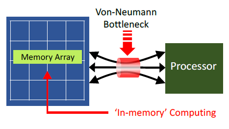
“AI is the new electricity.”, according to Andrew Ng, Professor at Stanford University. The potential applications for machine learning classification are vast. Yet, current ML inference techniques are limited by the high power dissipation associated with traditional architectures. The figure below highlights the von Neumann bottleneck. (A von Neumann architecture refers to the separation between program execution and data storage.)

The power dissipation associated with moving neural network data – e.g., inputs, weights, and intermediate results for each layer – often far exceeds the power dissipation to perform the actual network node calculation, by 100X or more, as illustrated below.

A general diagram of a (fully-connected, “deep”) neural network is depicted below. The fundamental operation at each node of each layer is the “multiply-accumulate” (MAC) of the node inputs, node weights, and bias. The layer output is given by: [y] = [W] * [x] + [b], where [x] is a one-dimensional vector of inputs from the previous layer, [W] is the 2D set of weights for the layer, and [b] is a one-dimensional vector of bias values. The results are typically filtered through an activation function, which “normalizes” the input vector for the next layer.

For a single node, the equation above reduces to:
yi = SUM(W[i, 1:n] * x[1:n]) + bi
For CPU, GPU, or neural network accelerator hardware, each datum is represented by a specific numeric type – typically, 32-bit floating point (FP32). The FP32 MAC computation in the processor/accelerator is power-optimized. The data transfer operations to/from memory are the key dissipation issue.
An active area of neural network research is to investigate architectures that reduce the distance between computation and memory. One option utilizes a 2.5D packaging technology, with high-bandwidth memory (HBM) stacks integrated with the processing unit. Another nascent area is to investigate in-memory computing (IMC), where some degree of computation is able to be completed directly in the memory array.
Additionally, data scientists are researching how to best reduce the data values to a representation more suitable to very low-power constraints – e.g., INT8 or INT4, rather than FP32. The best-known neural network example is the MNIST application for (0 through 9) digit recognition of hand-written numerals (often called the “Hello, World” of neural network classification). The figure below illustrates very high accuracy achievable on this application with relatively low-precision integer weights and values, as applied to the 28×28 grayscale pixel images of handwritten digits.
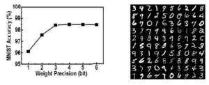
One option for data type reduction would be to train the network with INT4 values from the start. Yet, the typical (gradient descent) back-propagation algorithm that adjusts weights to reduce classification errors during training is hampered by the coarse resolution of the INT4 value. A promising research avenue would be to conduct training with an extended data type, then quantize the network weights (e.g., to INT4) for inference usage. The new inference data type values from quantization could be signed or unsigned (with an implicit offset).
IMC and Advanced Memory Technology
At the recent VLSI 2020 Symposium, Yih Wang, Director in the Design and Technology Platform Group at TSMC, gave an overview of areas where in-memory computing is being explored to support deep neural network inferencing.[1] Specifically, he highlighted an example of IMC-based SRAM fabrication in 7nm that TSMC recently announced.[2] This article summarizes the highlights of his presentation.
SRAM-based IMC
The figure below illustrates how a binary multiply operation could be implemented in an SRAM. The “product” of an input value and a weight bit value is realized by accessing a wordline transistor (input) and a bit-cell read transistor (weight). Only in the case where both values are ‘1’ will the series device connection conduct current from the (pre-charged) bitline, for the duration of the wordline input pulse.
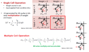
In other words, the ‘1’ times ‘1’ product results in a voltage change on the bitline, dependent upon the Ids current, the bitline capacitance, and the duration of the wordline ‘1’ pulse.
The equation for the output value yi above requires a summation across the full dimension of the input vector and a row of the weight matrix. Whereas a conventional SRAM memory read cycle activates only a single decoded address wordline, consider what happens when every wordline corresponding to an input vector bit value of ‘1’ is raised. The figure above also presents an equation for the total bitline voltage swing as dependent on the current from all (‘1’ * ‘1’) input and weight products.
Another view of the implementation of the dot product with an SRAM array is shown below. Note that there are two sets of wordline drivers – one set for the neural network layer input vector, and one set of for normal SRAM operation (e.g., to write the weights into the array).
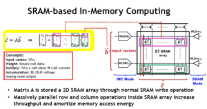
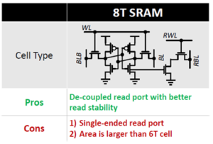
Also, the traditional CMOS six-transistor (6T) bit cell is designed for a single active wordline (with restoring sense amplification for data and data_bar). For the dot product calculation where many input wordlines could be active, an 8T cell with separate Read bitline from Write bitlines is required – the voltage swing equation above applies to the current discharging this distinct Read bitline.
The figures above are simplified, as they illustrate the vector product using ‘1’ or ‘0’ values. As mentioned earlier, the quantized data types for low power inference are likely greater than one bit, such as INT4. The implementation used by TSMC is unique. The 4-bit value of the input vector entry is represented as a series of 0 to 15 wordline pulses, as illustrated below. The cumulative discharge current on the Read bitline represents the contribution from all input pulses on each wordline row.
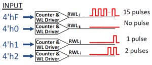
The multiplication product output is also an INT4 value. The four output signals use separate bitlines – RBL[3] through RBL[0] – as shown below. When the product is being calculated, the pre-charged bitlines are discharged as described above. The total capacitance on each bitline is the same – e.g., “9 units” – the parallel combination of the calculation and compensation capacitances.
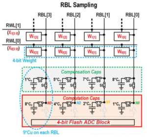
After the bitline discharge is complete, the compensation capacitances are disconnected. Note the positional weights of the computation capacitances – i.e., RBL[3] has 8 times the capacitance of RBL[0]. The figure below shows the second phase of evaluation, when the four Read bitlines are connected together. The “charge sharing” across the four line capacitances implies that the contribution of the RBL[3] line is 8 times greater than RBL[0], representing its binary power in a 4-bit multiplicand.

In short, a vector of 4-bit input values – each represented as 0-15 pulses on a single wordline—is multiplied against a vector of 4-bit weights, and the total discharge current is used to produce a single (capacitive charge-shared) voltage at the input to an Analog-to-Digital converter. The ADC output is the (normalized) 4-bit vector product, which is input to the bias accumulator and activation function for the neural network node.
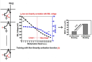
Yih highlighted the assumption that the bitline current contribution from each active (‘1’ * ‘1’) product is the same – i.e., all active series devices will contribute the same (saturated) current during the wordline pulse duration. In actuality, if the bitline voltage drops significantly during evaluation, the Ids currents will be less, operating in the linear region. As a result, the quantization of a trained deep NN model will need to take this non-linearity into account when assigning weight values. The figure below indicates that a significant improvement is classification accuracy is achieved when this corrective step is taken during quantization.
IMC with Non-volatile Memory (NVM)
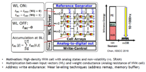
In addition to using CMOS SRAM bit cells, Yih highlighted that an additional area of research is to use a Resistive-RAM (ReRAM) bit cell array to store weights, as illustrated below. The combination of an input wordline transistor pulse with a high-R or low-R resistive cell defines the resulting bitline current. (ideally, the ratio of the high resistance state to the low resistance state is very large.) Although similar to the SRAM operation described above, the ReRAM array would offer much higher bit density. Also, further fabrication research into the potential for one ReRAM bit cell to have more than two non-volatile resistive states offers even greater neural network density.
Summary
Yih’s presentation provided insights into how the architectural design of memory arrays could readily support In-Memory Computing, such as the internal product of inputs and weights fundamental to each node of a deep neural network. The IMC approach provides a dense and extremely low-power alternative to processor plus memory implementations, with the tradeoff of quantized data representation. It will be fascinating to see how IMC array designs evolve to support the “AI is the new electricity” demand.
-chipguy
References
[1] Yih Wang, “Design Considerations for Emerging Memory and In-Memory Computing”, VLSI 2020 Symposium, Short Course 3.8.
[2] Dong, Q., et al., “A 351 TOPS/W and 372.4 GOPS Compute-in-Memory SRAM Macro in 7nm FinFET CMOS for Machine-Learning Applications”, ISSCC 2020, Paper 15.3.
Also, please refer to:
[3] Choukroun, Y.., et al., “Low-bit Quantization of Neural Networks for Efficient Inference”, IEEE International Conference on Computer Vision, 2019, https://ieeexplore.ieee.org/document/9022167 .
[4] Agrawal, A., et al., “X-SRAM: Enabling In-Memory Boolean Computations in CMOS Static Random Access Memories”, IEEE Transactions on Circuits and Systems, Volume 65, Issue 12, December, 2018, https://ieeexplore.ieee.org/document/8401845 .
Images supplied by the VLSI Symposium on Technology & Circuits 2020.
Share this post via:



Comments
5 Replies to “In-Memory Computing for Low-Power Neural Network Inference”
You must register or log in to view/post comments.