
PCIe, or peripheral component interconnect express, is a very popular high-speed serial computer expansion bus standard. The width and speed the standard supports essentially defines the throughput for high-performance computing (HPC) applications. The newest version, PCIe 6.0 promises to double the bandwidth that the current PCIe 5.0 specification offers. The standard is still a bit away from full release and mainstream deployment, but it is a highly anticipated technology that promises to set new benchmarks for performance throughout the industry. Samtec and Synopsys have teamed up to present a very interesting webinar on the topic. Read on to learn the backstory of PCIe 6.0 for HPC, from IP to interconnect.
Any high-speed communication channel requires two primary ingredients, IP to process the signals and a physical medium to deliver those signals. In a past life, my company developed high-speed SerDes (serializer/deserializer) IP. We are quite proud of its capabilities to deliver robust signals at high speed over long distances. Those were just academic projections until we teamed up with Samtec. They developed a high-precision copper cable that was several meters long. That medium really allowed to prove our point and we turned heads at many trade shows with the demo we created with Samtec.
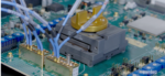
The Demo
Similarly, an early PCIe 6.0 implementation requires IP to process the signals, a physical signal path and a set of stimuli to show what can be achieved. In this context, Synopsys provides the PCIe 6.0 IP and Samtec provides the physical connectivity and signal activity. A rather impressive demo has been developed to showcase what can be achieved with this emerging standard. The demo has been shown live recently at DesignCon, AI Hardware Summit, and most recently at Supercomputing (SC21). Note Samtec has a history of interesting demos at DesignCon. A video of this demo will be shown during the webinar. While quite interesting, this is not the main benefit of attending the webinar. More on that in a moment. First, a summary of the demo.
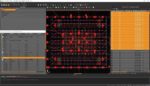
Thanks to its new DesignWare IP for PCIe 6.0, the Synopsys PHY generates four 64 GT/s PAM4 differential signals (PCIe 6.0 data rate). The differential pairs route through an Isola Tachyon® 100 G test board, to a Samtec 70 GHz Bulls Eye® High-Performance Test System cable assembly, the BE-70A Series. The signal travels from the Bulls Eye connector, through 8” of low-loss coax cable, to precision 1.85 mm Samtec compression mount jacks, mounted on the first HSEC6 SI Evaluation Board.
The signals then travel about 30 mm in the board to the HSEC6 connector, and then to the second evaluation board. The differential pair exits the second evaluation board through another set of 1.85 mm compression mount jacks, through another 8” of coax cables, and are received back to the Bulls Eye test cable system, on the Synopsys board. The data routes back to and is recovered by the Synopsys PCIe receiver.
The results of the demo are eye-popping. During the webinar, you will learn all about bit error rates and see the eye diagrams. While impressive, there is a lot more to learn by attending this webinar.
The Backstory
This demonstration vehicle is one of the first interoperability platforms for PCIe 6.0 in the industry. There is much to be learned here, including practical signal channel design techniques and connectivity options. These are nuggets that are hard to get in a trade show environment. You need 1:1 access to experts who have the time to discuss the details. This is what you will get in this webinar.
The webinar is presented by two technology experts. Matthew Burns presents for Samtec. Over the course of 20+ years, he has been a leader in design, technical sales and marketing in the telecommunications, medical and electronic components industries. Mr. Burns holds a B.S. in Electrical Engineering from Penn State University.
Madhumita Sanyal presents for Synopsys. She has over 16 years of experience in design and application of ASIC WLAN products, logic libraries, embedded memories, and mixed-signal IP. Madhumita holds a Master of Science degree in Electrical Engineering from San Jose State University and LEAD from Stanford Graduate School of Business.
The webinar will be held on Wednesday, December 8, 2021, from 10:00 AM – 11:00 AM Pacific Standard Time. You can register here. If PCIe 6.0 is in your future this is a great opportunity to get a head start. Seeing a demo at a trade show is useful but getting the details of what is happening behind the scenes and what design considerations are important can be invaluable. Now you know the backstory of PCIe 6.0.


