
The next design revolution is clearly upon us. Traditional Moore’s Law is slowing, but the exponential demand for innovation and form factor density is not. When you can no longer get it done with a single monolithic chip, moving to a multi-die approach is the answer. This emerging design methodology has many challenges – supply chain-oriented, materials-oriented, and standards-oriented to name a few. There is promising innovation from EDA, IP and standards organizations. Sitting above all this work is a substantial challenge. With so many options to implement new system-level silicon, which set of options are best? 2.5D, 3D, technology choices, IP/chiplet choices and so on. It’s a vexing problem since starting with the wrong options can lead to huge cost and schedule impact. The problem has been referred to as pathfinding, and that is the topic of this post. Read on to see how MZ Technologies is making multi-die design a reality.
About MZ Technologies
I mentioned pathfinding. In the context here, the term refers to identifying the optimal technology choices to implement a 2.5D or 3D multi-die design. The problem has been around for quite a while. Here is a discussion of it from the 2009 IEEE International Symposium on System-on-Chip. I have some experience with these problems as well. Around this same time frame while I was at Atrenta, we developed an early tool to address the pathfinding problem. And later, while at eSilicon, I got an up-close look at how challenging 2.5D design can be.
MZ Technologies was founded in 2014 by a team of leading EDA, IC, and package co-design experts. The goal was to build new technology from scratch to deal with the I/O planning and optimization phase of the physical implementation of complex 2.5D and 3D integrated circuits. That is, solve the pathfinding problem. A bit about the name of the company, which is shorthand for monozukuri. In Japanese, “monozukuri” is a compound word comprising “mono”, which literally means “things” (“products”), and “zukuri”, which means “process of making” or “creation”.
The company is a European EDA provider delivering GENIO™ a unified cockpit for 2.5D & 3D chiplet-based system design. GENIO is a tool that fills the pathfinding gap for multi-die design. It doesn’t compete with existing technologies, but rather interfaces with them to create a broader, more holistic capability. The tool has been around through several releases and has seen application across a wide range of multi-die designs. More on that in a bit.
What MZ Technologies Does
GENIO addresses the system architecture and IC/package co-development flow. This is the part of the design process that typically sits above existing tools and IP. It answers critical questions about the best implementation approach from a form factor, energy, performance, and cost point of view. Getting these things right early in the process can be the margin of victory for a complex design. Starting with a sub-optimal approach will create re-work, overruns, and a good chance the project will fail.
The figure below shows how GENIO fits into the overall design flow with existing tools.
The tool fits in the flow from concept to design to deliver a first time right optimal result. The goal is to create better manufacturability with optimal resources usage and better yield. GENIO works across the complete design ecosystem from silicon to package to PCB, with integrated design flows.
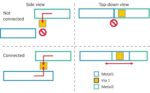
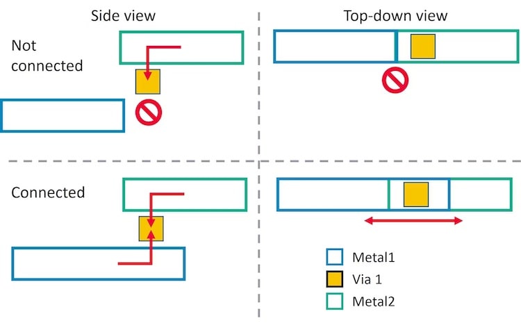
Digging a bit deeper, system architecture exploration is supported for planning, implementation, and analysis across different engineering domains. What-if analysis is provided for 2D, 2.5D and 3D interconnect management, I/O planning, and optimization. For example, planar vs. SI-based vs. 3D-stack. The optimization algorithms tame multi-die design computational complexity. Early estimations of electrical, mechanical, and thermal behavior are also provided.
With GENIO, it is possible to optimize in one shot through the full system hierarchy, from the top level to subsystems and components. A sophisticated GUI allows cross-highlight and scripting, among other functions, with the ability to go back in the design history to tag the most promising configurations. The figure below shows an example of the GUI.
GENIO has delivered a remarkable 60x reduction of architectural design time. The table below illustrates the types of designs GENIO has been applied to.
Here is a summary of the current version and next generation of the tool:
GENIO V1.x (commercially available today with a back-end orientation)
- Comprehensive system view spans the entire design ecosystem
- Cross-fabric platform, integrated with traditional IC, package & PCB design tools
- System-level architecture exploration
- Identifies the more efficient and cost-effective option into 3D system offering
- Single, consistent Interconnect Manager
- Represent and maintain the 3D model of the entire system
- Cross-hierarchical 3D-aware pathfinding
- Constraint-driven, proprietary optimization algorithms
- 3D chiplet-based design flow with multiple IP libraries
- Die stacking and silicon-to-silicon vertical communications – mix-and-match “LEGO-like” assembly
GENIO EVO (Next Evolution release; introduces simulation-aware optimization)
- Complete 3D system view across physical implementation and analysis
- Super-fast parasitic estimation for early analysis
- What-if analysis before physical implementation starts
- State-of-the-art TSV modeling
- Including electrical performance (R/C) and mechanical/thermal behavior
- Thermal modeling
- Based on power dissipation map and TSVs contribution
- Mechanical stress
- Voltage and temperature monitor placement according to identified thermal hotspots
- Critical net group spotting and prioritization
- 3DBlox language support
- 3D-system partitioning flow
- Support to system partitioning in the early stages of RTL & synthesis
- 3D-stack floor planning
- Best positioning of system components/chiplets across the stack planes
To Learn More
MZ Technologies licenses its software with a time-based model. Additional services for custom integration, custom module development, and customer training are also available. If you are planning to tackle a multi-die design, you should contact them. I can tell you from first-hand experience the problem MZ solves is very real and can become a fatal flaw if not addressed early. You can reach out at info@monozukuri.eu. And that’s how MZ Technologies is making multi-die design a reality.
Also Read:
Outlook 2024 with Anna Fontanelli Founder & CEO MZ Technologies


