While I was in Taiwan last month battling a Super Typhoon, Morris Chang was in Silicon Valley picking up his IEEE Medal of Honor. Gordon Moore, Andrew Grove, and Robert Noyce all have medals. The other winners, including 10 Nobel prize recipients, are listed HERE. An updated wiki on Dr. Morris Chang is located HERE.
The 12+ hour plane ride home gives a person plenty of time for reflection on why TSMC is so successful. Leadership is certainly important, just take a look at the executive staff on the new TSMC corporate website ( www.tsmc.com ). But in my opinion, TSMC’s success boils down to one thing, they are a dedicated IC foundry that is dependent on its customers and ecosystem partners and TSMC has never forgotten that.
Foundry 2010 Revenues:
(1) TSMC $13B
(2) UMC $4B
(3) GFI $3.5B
(4) SMIC $1.5B
(5) Dongbu $512M
(6) Tower/Jazz $509M
(7) Vanguard $508M
(8) IBM $430M
(9) Samsung $420M
(10) MagnaChip $405M
But if you ask how TSMC and Dr. Morris Chang himself got where they are today it can be summed up in three words: Business Model Innovation. Other business model innovators include: eSilicon, ARM, Apple, Dell, Starbucks, Ebay, Google, etc…. I would argue that without TSMC some of these businesses would not even exist.
Morris Chang’s education started at Harvard but quickly moved to MIT as his interest in technology began to drive his future. From MIT mechanical engineering graduate school Morris went directly into the semiconductor industry at the process level and was quickly moved to management. After completing an electrical engineering PhD program at Stanford, Morris leveraged his process level semiconductor management success and went to Taiwan to head the Industrial Technology Research Institute (ITRI) which lead to the founding of TSMC.
In 1987 TSMC started 2 process nodes behind current semiconductor manufacturers (IDMs). Morris Chang made the first TSMC sales calls with a single brochure: TSMC Core Values: Integrity, commitment, innovation, partnership. 4-5 years later TSMC was only behind 1 node and the orders started pouring in. In 10 years TSMC caught up with IDMs (not Intel) and the fabless semiconductor industry blossomed enabling a whole new era of semiconductor design and manufacturing.
Morris Chang Awards
- 1998, “Top 25 Managers of the Year” and “Stars of Asia” by Business Week.
- 1998, “One of The Most Significant Contributors in the 50 years of Semiconductor Industry” by BancAmerica Robertson Stephens.
- 2000, “IEEE RobertN. Noyce Award” for Exceptional Contributions to Microelectronics Industry.
- 2000, “Exemplary Leadership Award” from the Fabless Semiconductor Association (GSA).
- 2005, “Top 10 Most Influential Leaders of the World” by Electronic Business.
- 2008, “Semiconductor Industry Association’s Robert N. Noyce Award”
- 2009, “EE Times Annual Creativity in Electronics Lifetime Achievement Award”
- 2011, IEEE Medal of Honor
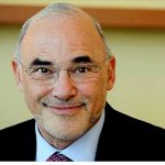
Dr. Morris Chang turned 80 on July 10[SUP]th[/SUP] 2011, I have seen him in Fab 12 but we have not met. Morris returned to the CEO job in June of 2009 and is still running TSMC full time as CEO and Chairman. He works from 8:30am to 6:30pm like most TSMC employees and says that a successful company life cycle is: rapid expansion, a period of consolidation, and maturity. The same could be said about Morris himself.
Here is a new 5 minute video from TSMC. I highly recommend watching it:
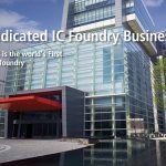
Pioneer of Dedicated IC Foundry Business Model
Related Blogs:TSMC 28nm / 20nm Update!