The TSMC Open Innovation Platform (OIP) Ecosystem Forum has become the industry benchmark when it comes to showcasing industry-wide collaboration. The extreme design, integration and packaging demands presented by multi-die, chiplet-based design have raised the bar in terms of required collaboration across the entire supply chain. World-class development and collaboration were on display at the recent event, which was held in Santa Clara on September 25, 2024. A critical technology required for success is enabling IP, in particular for sensing and power management. Analog Bits showcased substantial capabilities here. Let’s examine some of the work presented to see how Analog Bits builds a road to the future at TSMC OIP.
IP Development Progress
Analog Bits discussed some of the unique challenges advanced chip and multi-die design presents. Multi-domain sensing was discussed, along with the additional challenge of non-uniform thermal distributions. Real-time monitoring is another requirement. If the face of all this, calibration complexity, voltage supply noise, and crosstalk must all be dealt with as well.
Analog Bits portfolio of on-die sensing IP was presented, including:
- PVT Sensors – integrated and pinless
- Power on reset and over current detection macros
- Power supply detectors that include:
- Fast detecting glitch
- Synchronized droop detection with filtering and differential sensing
The benefits of a comprehensive on-die sensing IP portfolio were also discussed. At the top of the list is improved power efficiency. A good approach here also prevents overheating and minimizes thermal stress. The overall benefits of enhanced reliability and improved yield also come into play.
Power management is also a key benefit. Things like voltage scalability, voltage spike, and droop protection are examples. Better integration that results in space savings is an added benefit.
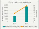
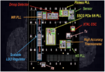
Analog Bits presented a significant amount of silicon data based on a TSMC N3P test chip. The graphic at the stop of this post is an overview of what’s on this chip. There were many impressive results to show. Here is a list of some of them:
- Temperature linearity and precision for the High-Accuracy Thermometer
- Linearity and precision for the high-accuracy Voltage Sensor
- Measured trigger voltage vs. threshold and untrimmed threshold accuracy for the Droop Detector
- An overview of Low-Dropout (LDO) regulator development
Regarding the LDO, here is a summary of the program:
- First LDO modules proven in silicon
- Latest N3 test-chip taped out Q2 2024
- Packaging and initial bring up Q1 2025
- Automotive planned for mid-2025
Here is an example of the data presented. The plot is showing Voltage Sensor accuracy with the following parameters: VDDA: 1.2V, VDD: 0.75V, Corner: TT.
IP Collaboration Progress
OIP is all about ecosystem collaboration, so Analog Bits teamed with Arm to present an impressive presentation entitled, Optimized Power Management of Arm CPU Cores with Integrated Analog Bits Power Management and Clocking IP’s. The presenters were Lisa Minwell, Director of Technology Management at Arm and Alan Rogers, President at Analog Bits.
The once-in-a-generation transformation occurring in digital infrastructure was discussed. Complexity increases in data center SoC’s, coupled with AI deployment has made energy efficiency a central issue. It was pointed out that advanced chip and chiplet-based designs in 3nm and 2nm are integrating many Arm Neoverse cores.
The need for managing power to these cores on a granular level is getting increasingly important. The traditional methods of using off-chip LDO and power sensors no longer scales. A new approach is needed.
The work Analog Bits and Arm have done on several integrated power management and clocking IPs was presented. Arm customers can readily use these solutions in N3P and soon in N2P. LDO regulator IPs were also discussed to efficiently manage the large absolute and dynamic current supplies to Arm CPU cores.
A case study of how CPU cores seamlessly integrate with Analog Bits LDO and Power Glitch Detector IPs, along with integrated clocking capabilities was also presented. The implications of this work is substantial for advanced data center applications.
To Learn More
I have presented some of the highlights of Analog Bits presence at TSMC OIP. There is a lot more to the story, and you find out more about Analog Bits industry impact on SemiWiki here. You can also check out the company’s website here. And that’s how Analog Bits builds a road to the future at TSMC OIP.