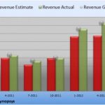
RVN! 26 Banner revised (800 x 100 px) (600 x 100 px)

Atrenta’s Spring Cleaning Deal

Atrenta’s Spring Cleaning Deal
by Paul McLellan on 04-16-2012 at 9:00 am

Atrenta is having a special offer to let you “spring clean” your IP for free. They are providing two weeks of free access to the Atrenta IP kit starting from today, April 16th, until the end of May. During this period, qualified design groups in the US will be able to use the kit for two consecutive weeks to “spring clean” their third party or internally developed IP blocks at no cost.

Atrenta’s IP Kit is also used by TSMC to quality soft IP for inclusion in the TSMC 9000 IP library. See my blog here. Plus it is TSMC’s technology symposium tomorrow.

The IP Kit generates two important reports: the Atrenta DashBoard and DataSheet.


The Atrenta DashBoard provides a pass/fail status for all IP blocks. It shows the status of the block for key design objectives such as CDC, power, test, timing constraints and more. It also reflects overall readiness of the IP as measured by various quality goals. User-defined success criteria are used to report tolerance to fatals, errors and warnings. Designers are able to drill down to get additional information on the exact violations reported, as well as access trend data that shows overall progress to achieve a passing status over time. A SpyGlass Clean report has no failures reported.


The second report is the Atrenta DataSheet. This report focuses on IP characteristics. Once the DashBoard report is “clean,” the DataSheet acts as a final handoff document that captures key information about the IP block, such as the I/O table, clock trees, reset trees, final power spec, test coverage, constraints coverage and more. Especially useful when a block is being integrated, the report gathers this key information into one easy-to-read HTML document.

And if you really get carried away with the idea of spring cleaning, my condo could do with some attention.

Details on the IP Kit Spring Cleaning promotion is here.

And Atrenta’s geek friend has his own take (1.5 mins):


High Yield and Performance – How to Assure?

High Yield and Performance – How to Assure?
by Pawan Fangaria on 04-16-2012 at 7:30 am

In today’s era, high performance mobile devices are asserting their place in every gizmos we play with and guess what enables them work efficiently behind the scene – it’s large chunks of memory with low power and high speed, packed as dense as possible. Ever growing requirement of power, performance and area led us to process nodes like 20nm, but that has a burgeoning challenge of extreme process variation limiting the yield. However there is no escape from detecting the failure rate early in the cycle to assure high yield.

In case of memory, there can be billions of bit cells with column selectors and sense amplifiers and you can imagine the read / write throughput on those cells. Although redundant columns and error correction mechanisms are provided, they are not sufficient to tolerate bit cell failure above a certain number. The requirement here is to detect failure in the range of sigma of 6.

So, how do we detect failure at such high precision? Traditional methods are mostly based on Monte Carlo (MC) simulation, the idea first invented by Stanislaw Ulam, John Neumann and Nicholas Metropolis in 1940. To get a feel of this, let’s consider a bit cell of 6 transistors with 5 process variables per device, making a total of 30 process variables. Below is the QQ plot of distribution of bit cell read current (cell_i) on x-axis and cumulative density function (CDF) on y-axis. Each dot on the graph is a MC sample point. There are 1 million samples simulated.


QQ plot of bit cell read current with 1M MC samples simulated

The QQ curve is a representation of the response of output to process variables. The bend in the middle of the curve means a quadratic response in that region. The sharp drop off in bottom left means a circuit cut off in that region. Clearly any method assuming linear response will be extremely inaccurate.

Now consider the QQ plot for delay of a sense amplifier having 125 process variables.


QQ plot of delay of sense amplifier with 1M MC samples simulated

The three stripes indicate three distinct sets of delays indicating discontinuities; a small step in process variable space sometimes leads to major change in performance. Such strong nonlinearities will make linear and quadratic models completely fail. It must also be noted that the above result is obtained after 1M MC samples which covers circuits of about 4-sigma. For 6-sigma, one would need about 1 billion MC samples, not practical.

In order to detect rare failures with lesser samples, many variants of MC method and other analytical methods have been tried, but each of them lacks in either of robustness, accuracy, practicality or scalability. Some of them can work with only 6 to 12 process variables. A survey of all of them is provided in a white paper by Solido Design Automation.

Solido has developed a new method; they call it HSMC (High Sigma Monte Carlo) which is promising; fast, accurate, scalable, verifiable and usable. This method has been implemented as a high quality tool in Solido Variation Designer Platform.

The HSMC method prioritizes simulations towards the most-likely-to-fail cases by adaptive learning through feedback from SPICE. It never rejects any sample in case it causes failure, hence increasing accuracy. The method can produce extreme tail of the output distributions (like in QQ plot), using real MC samples and SPICE accurate results in hundreds or a few thousand simulations. The flow goes something like this –

  • 1. Extract 6-sigma corners by simply running HSMC, opening the resulting QQ plot, selecting the point at the 6-sigma mark, and saving it as a corner.
  • 2. Bit cell or sense amplifier designs are tried with different sizing. For each candidate design, one only needs to simulate at the corner(s) extracted in the 1[SUP]st[/SUP] step. The output performances are at “6-sigma yield”, but only with a handful of simulations.
  • 3. Finally, verify the yield by doing another run of HSMC. The flow concludes if there are no significant interactions between process variables and outputs, which is generally the case. Otherwise, a re-loop is done, by choosing a new corner, designing against it and verifying.

Let’s look at the results of HSMC applied on the same bit cell and sense amplifier designs –


Bit cell_i – 100 failures in first 5000 samples


Sense amp delay – 61 failures in first 9000 samples


QQ plot of cell_i – 1M MC samples and 5500/100M HSMC samples
MC would have taken 100M samples against 5500 with HSMC


QQ plot of sense amp delay – 1M MC samples and 5500/100M HSMC samples

The process is extended further for reconciliation between global (die-to-die, wafer-to-wafer) and local (within-die) statistical process variation. It is clear that this method is fast due to handful of samples to be simulated, accurate as no likely failure is rejected, scalable as this method can handle 100s of process variables, verifiable and usable.

The details can be looked into the actual white paper, “High-Sigma Monte Carlo for High Yield and Performance Memory Design”, written by Trent McConaghy, Co-founder and CTO, Solido Design Automation, Inc.

By Pawan Kumar Fangaria
EDA/Semiconductor professional and Business consultant
Email:Pawan_fangaria@yahoo.com


Making your ARMs POP

Making your ARMs POP
by Paul McLellan on 04-16-2012 at 6:30 am

Just in time for TSMC’s technology symposium (tomorrow) ARM have announced a whole portfolio of new Processor Optimization Packs (POPs) for TSMC 40nm and 28nm. For most people, me included, my first question was ‘What is a POP?’

A POP is three things:

  • physical IP
  • certified benchmarking
  • implementation knowledge

Basically, ARM takes their microprocessors, which are soft cores, and implements them. Since so many of their customers use TSMC as a foundry, the various TSMC processes are obviously among the most important. They examine the critical paths and the cache memories and design special standard cells and other elements to optimally match the processor to the process. They don’t do this just once, they pick a few sensible implementation choices (highest performance 4 core for networking, medium performance dual core for smartphones, lowest power single core for low end devices). A single POP contains all the components necessary for all these different power/performance/area points. Further, although we all casually say things like ‘TSMC 40nm’ in fact TSMC has two or three processes at each node to hit different performance/power points, so they have to do all of this several times.

Then they provide the performance benchmarks that they managed to achieve, along with all the detailed implementation instructions as to how they did it. These are EDA tool chain independent since customers have different methodologies. But the combination of IP and documentation should allow anyone to reproduce their results or get equivalent results with their own implementations after any changes that they have made for their own purposes and to differentiate themselves from their competitors.

Companies using the POPs get noticeably better results than simply using the regular libraries and doing without the specially optimized IP.

About 50% of licensees of the processors for which POPs have been available seem to have licensed them, currently there are 28 companies using them. Here’s a complete list of the POPs (click to enlarge):
Of course ARM has new microprocessors in development (for example, the 64 bit ones already announced) and they are also working closely with foundries at 20nm and 14nm (including FinFETs). So expect that when future microprocessors pop out that a POP will pop out too.

About TSMC

TSMC created the semiconductor Dedicated IC Foundry business model when it was founded in 1987. TSMC served about 470 customers and manufactured more than 8,900 products for various applications covering a variety of computer, communications and consumer electronics market segments. Total capacity of the manufacturing facilities managed by TSMC, including subsidiaries and joint ventures, reached above 9 million 12-inch equivalent wafers in 2015. TSMC operates three advanced 12-inch wafer GIGAFAB™ facilities (fab 12, 14 and 15), four eight-inch wafer fabs (fab 3, 5, 6, and 8), one six-inch wafer fab (fab 2) and two backend fabs (advanced backend fab 1 and 2). TSMC also manages two eight-inch fabs at wholly owned subsidiaries: WaferTech in the United States and TSMC China Company Limited, In addition, TSMC obtains 8-inch wafer capacity from other companies in which the Company has an equity interest.

TSMC’s 2015 total sales revenue reached a new high at US$26.61 billion. TSMC is headquartered in the Hsinchu Science Park, Taiwan, and has account management and engineering service offices in China, Europe, India, Japan, North America, and, South Korea.


The Truth of TSMC 28nm Yield!

The Truth of TSMC 28nm Yield!
by Daniel Nenni on 04-15-2012 at 7:00 pm

As I write this I sit heavyhearted in the EVA executive lounge returning from my 69[SUP]th[/SUP] trip to Taiwan. I go every month or so, you do the math. This trip was very disappointing as I can now confirm that just about everything you have read about TSMC 28nm yield is absolutely MANURE!
Continue reading “The Truth of TSMC 28nm Yield!”


Arteris evangelization High Speed Interfaces!

Arteris evangelization High Speed Interfaces!
by Eric Esteve on 04-15-2012 at 4:36 am

Kurt Shuler from Arteris has written a short but useful blog about the various high speed interface protocols currently used in the wireless handset (and smartphone) IP ecosystem. Arteris is well known for their flagship product, the Network-on-Chip (NoC), and the Mobile Application Processor market segment represent the first target for NoC: NoC is the IP which help increasing overall chip performance by optimizing internal interconnect, allows avoiding routing congestion during Place & Route and finally helps SoC design team integrating more quickly the tons of various functions, such an IP is more than welcome in such a competitive IC market segment! To make it clear, NoC is supporting interconnects inside the chip, when Kurt’s blog deals with the various functions used to interface the SoC with the other IC, still located inside the system (smartphone or media tablet). The blog provides a very useful summary, under the form of a table listing the various features of: MIPI HIS (High Speed Interface), USB HSIC (High Speed Inter-Chip), MIPI UniPro & UniPort, MIPI LLI (Low Latency Interface) and C2C (Chip-To-Chip Link).

We will come back later on the listed MIPI specifications and USB HSIC, but I would like to highlight the last two in the list: LLIand C2C.

The first is based on high speed serial differential signaling and require using MIPI M-PHY physical block when the second is a parallel interface and requiring only LPDDR2 I /Os, but both functions are used in the aim of sharing a single memory (DRAM) between two chips, usually the application processor and the modem. The result is that the system integrator will save 2$ in the bill of material (BOM)… It does not look so fantastic, until you start multiplying these two bocks by the number of systems built by an OEM. Just multiply several dozens of million by 2$ and you realize that the return on investment (the additional cost of the C2C or LLI IP license) can come very fast, and represent several dozen of million dollar!

I should also add that Arteris is marketing these both controller IP functions, and if the company has the full rights on C2C, LLI is one of the numerous MIPI specifications. Just to give you some insight, LLI has been originally developed by one of the well known application processor chip makers, then the company has offered LLI to MIPI alliance and has asked Arteris to turn this internally developed function into a marketable IP, that Arteris is doing with an undisputable success. As far as I am concerned, I think that both LLI and C2C are “self selling”, as soon as you know that you can save $2 on the system BOM, you can imagine that OEM are pushing hard the chip makers to integrate such a wonderful function!
About Arteris
Arteris provides Network-on-Chip (NoC) interconnect semiconductor intellectual property (IP) to System on Chip (SoC) makers so they can reduce cycle time, increase margins, and easily add functionality. Arteris invented the industry’s first commercial network on chip (NoC) SoC interconnect IP solutionsand is the industry leader. Unlike traditional solutions, Arteris interconnect plug-and-play technology is flexible and efficient, allowing designers to optimize for throughput, power, latency and floorplan.

To know more about MIPI, you can visit:

MIPI Alliance web

MIPI wikion Semiwiki

MIPI surveyon IPNEST

Reminder: for Kurt’s blog, just go here!

Eric Esteve from IPNEST


Handsets, what’s up?

Handsets, what’s up?
by Paul McLellan on 04-13-2012 at 3:02 pm

So who’s in and who’s out these days in handsets?

It looks as if Samsung has finally achieved a long-held goal to be the largest handset vendor, taking over from Nokia which has been the market leader for 14 years since 1998 when it passed Motorola. Nokia hasn’t reported yet but they cut their forecast. Samsung had a record quarter. Bloomberg estimates that Samsung sold 44M smart phones in Q1, and 92M phones in total, easily beating 83M for Nokia. Samsung also have a goal to be number one in semiconductor and overtake Intel, which they may well do but not immediately.

Nokia, as I’m sure you know, is largely betting its future on Microsoft and, in the US, on AT&T. It launched its new Lumia phone over easter weekend (when most AT&T stores were closed, not exactly like an iPhone lanuch with people camped out overnight to get their hands on the new model). There were also technical glitches about not being able to connect to the internet, which is a pretty essential feature for a smartphone. My own prediction is that WP7 is too little, too late and as a result Nokia is doomed. But maybe I underestimate the desperate need of the carriers to have an alternative to Android and iPhone that is more under their own control.

Funny isn’t it to look back just 8 or 10 years to when the carriers were paranoid about Microsoft, worrying that it might do to them in phones what they did to PC manufacturers where they took all the money (well, Intel got some too)? In the end it seems that it is then-tiny-market-share Apple that is taking all the money, 1/2 of the entire handset profits by some reports. iPhone alone is bigger than the whole of Microsoft. Samsung is also making good money but all the other smartphone handset makers such as HTC seem to be struggling. Now Microsoft is seen as the weakling, able to be bullied around the schoolyard by the carriers.

I still don’t entirely understand Google’s Android strategy. This quarter, for the first time, over 50% of new smartphones were Android based but Google makes very little from each one and all that is in incremental search. Like the old joke about if all you have is a hammer everything looks like a nail, every business seems to look like search to Google. Amazon is certainly making money with Android, and so is Samsung. There are rumors that Microsoft makes more than Google (through patent licenses to the major Android handset and tablet manufacturers). It remains to be seen what Google does with Motorola Mobility. If it favors them too much it risks alienating its other partners and pushing them away from Android. If it doesn’t favor them at all I don’t see why they should suddenly become a market leader in smartphones.

iPhone5 is expected in June or July. Presumably containing the quad-core A6. Presumably with LTE like the new iPad. But, of course, Apple isn’t saying anything.


Chip in the Clouds – "Gathering"

Chip in the Clouds – "Gathering"
by Kalar Rajendiran on 04-13-2012 at 1:29 pm


Cloud computing is the talk of the tech world nowadays. I even hear commentaries about how entrepreneurs are turned down by venture capitalists for not including a cloud component into their business plan no matter what the core business may be. The commentary goes “It’s cloudy without any clouds.” Add some clouds to your strategy and the future will be bright and sunny.

With such a strong trend, one might have expected companies within the $300B semiconductor market to have adopted “cloud” into their strategies by now and the answer is yes to varying degrees. Large established semiconductor companies as well as semiconductor value chain producer companies have built their enterprise-wide clouds for their engineers to tap into their vast compute farm. But access to the right number of latest and greatest compute resources may not always be available for the task on hand, independent of the size of the compute farm. This is because the compute farm is typically upgraded with new hardware resources on an incremental basis. So although the engineers may have their own private clouds to address the chip design needs, peak-time compute resource needs are not addressed optimally. And then there is the matter of peak-time EDA tools resource. Companies are still limited by the number of EDA tools licenses they own. If you’re a major customer of an EDA tools supplier, it is not an issue as peak-load license needs are addressed through temp licenses or short-term licenses. For everyone else, it is a painful negotiation with their EDA tools supplier. As much planning as can be done, peak-load needs cannot always be predicted well ahead of time. And the longer the negotiation with the EDA supplier takes, the more the customer falls behind on their tapeout schedule and consequently time-to-market schedule.

In other words, today, large to medium sized semiconductor companies have a private cloud for their compute needs and a kludge solution for their EDA license needs given their stature with their EDA suppliers. This solution has many issues. (1) they don’t need to maintain their compute servers but they do only to ensure they have access to compute power on-demand (2) they don’t have an automatic solution to add EDA tools resources on-demand (3) if using an EDA tools supplier’s cloud, customers don’t have a seamless cloud-based design flow simply because the design flow involves tools from more than one supplier.

As for smaller semiconductor companies, they neither have their own private cloud nor do they have the same flexible access to EDA tools licenses on-demand. And if using an EDA tools supplier’s cloud, they face the same issue as the larger customers do.

If a secure cloud-based chip design platform from a third-party company provides EDA suppliers agnostic, seamless design flow where the customer could tap into one particular set of tools for one chip project and a different set of tools (as per their team needs/skills) for a different chip project, that would be the ultimate offering. That ultimate offering is what would be called “Chip in the Clouds” platform.

“Chip in the Clouds” may have sounded a lot like “Head in the clouds.” But it is not. The time has arrived for “Chip in the clouds” platform to play a key role in redefining how chips are designed and implemented. Why do I say this? Stay tuned for future installments of my blog in which I’ll discuss the driving factors for the adoption as well as what is happening in the platform offering space.

http://www.linkedin.com/in/kalarrajendiran


I Love DAC

I Love DAC
by Paul McLellan on 04-13-2012 at 1:16 pm

For the fourth year Atrenta, Cadence and Springsoft are jointly sponsoring the “I LOVE DAC” campaign. In case you have been hibernating all winter, DAC is June 3-7th in San Francisco at the Moscone Center.

There are two parts to “I LOVE DAC”. First, if you register by May 15th (and they haven’t all gone) then you can get a free 3-day exhibit pass for DAC. In fact this pass entitles you not just to the exhibits but also the pavilion panels (which take place in the exhibit hall), the three keynotes and the evening receptions after the show closes.

Secondly, if you go to the Atrenta, Cadence or Springsoft booths you can get an “I LOVE DAC” badge. Each day somebody who is walking the show floor wearing one of the badges will be randomly given a new iPad (aka, but not by Apple, as iPad3). If you still have an “I LOVE DAC” from the previous 3 years then you can wear that one and still be eligible.

The “I LOVE DAC” page on the DAC website, where you can register, is here.


EDPS: 3D ICs, part II

EDPS: 3D ICs, part II
by Paul McLellan on 04-12-2012 at 10:00 pm

Part I is here.

In the panel session at EDPS on 3D IC a number of major issues got highlighted (highlit?).

The first is the problem of known-good-die (KDG) which is what killed off the promising multi-chip-module approach, perhaps the earliest type of interposer. The KDG problem is that with a single die in a package it doesn’t make too much sense to invest a lot of money at wafer sort. If the process is yielding well, then identify the bad die cheaply and package up the rest. Some will fail final test due to bonding and other packaging issues, and some die weren’t good to begin with (so you are chucking out a bad die after having spent a bit too much on it). With a stack just 4 die and a wafer sort that is 99% effective (only 1% of bad die get through), the stack only yields 95% and those 5% discarded do not just contain bad die, there are (almost) 3 good die and an expensive package too. Since these die are not going to be bonded out, they don’t automatically have bond pads for wafer sort to contact and it is beyond the state of the art to put a probe on a microbump (and at 1gm of force on 20um bump, that is enormous pressure) so preparing for wafer sort requires some thought.

The next big problem is who takes responsibility for what, in particular, when a part fails who is responsible. Everyone is terrified of the lawyers. The manufacturing might be bad, the wafer test may be inadequate, the microbumping assembly may be bad, the package may be bad and, generally, assigning responsibility is harder. It looks likely that there will end up being two manufacturers responsible, the foundry who does the semiconductor manufacturing, the TSV manufacturing and (maybe) the microbumps. And the assembly house or OSAT as we are now meant to call them (outsourced semiconductor assembly and test) who puts it all together and does final test.

The third big problem is thermal analysis. Not just the usual how hot does the chip get and how does that affect performance. But there are different thermal coefficients of expansion which can cause all sorts of mechanical failure of the connections in the stack. This was one of the biggest challenges in getting surface mount technology for PCBs to work reliably: the parts kept falling off the board due to the different reaction to thermal stresses. Not good if it was in your plane or car.

Philip Marcoux had a quote from the days of surface mount: “successful design and assembly of complex fine-pitch circuit boards is a team sport.” And 3D chips obviously are too. The team is at least:

  • the device suppliers (maybe more than one for different die, maybe not)
  • the interposer designer and supplier (if there is one)
  • the assembler
  • the material suppliers (different interconnects, different TSVs, different device thicknesses will need different materials, solder, epoxy…)
  • an understanding pharmacist or beverage supplier (to alleviate stresses)

His prescription for EDA:

  • develop a better understanding of the different types of TSV (W vs Cu; first/middle/last etc)
  • coordinate with assembly equipment suppliers to create an acceptable file exchange for device registration and placement
  • create databases of design guidelines to help define the selection of assembly processes, equipment and materials
  • encourage and participate in the creation of standards
  • develop suitable floorplanning tools for individual die
  • develop 3D chip-to-chip planning tools
  • provide thermal planning tools (chips in the middle get hot)
  • provide cost modeling tools to address designer driven issues such as when to use 3D vs 2.5D interposer vs big chip

It is unclear to me whether these are all really the domain of EDA. Process cost modeling is its own domain and not one where EDA is well-connected. Individual semiconductor companies and assembly houses guard their cost models as tightly as their design data.

Plus one of the challenges with standards is when to develop them. Successful standards require that you already know how to do whatever is being standardized and as a result most successful standards start life as a de facto standard and then the known rough edges are filed off.

As always with EDA, one issue is how much money is to be made. EDA tools partially make money based on how valuable they are, but also largely by how many licenses large semiconductor companies need. In practice, the tools that make money either run for a long time (STA, P&R, DRC) or you sit in front of them all day (layout, some verification). Other tools (high level synthesis, bus register automation, floorplanning) suffer from what I call the “Intel only needs one copy” problem, that they don’t stimulate license demand in a natural way (although rarely in such an extreme way that Intel really only needs a single copy, of course).


Doing what others don’t do

Doing what others don’t do
by Paul McLellan on 04-12-2012 at 2:56 pm

Wally Rhines’ keynote at U2U, the Mentor users’ group meeting, was about Mentor’s strategy of focusing on what other people don’t do. This is partially a defensive approach, since Mentor has never had the financial firepower to have the luxury of focusing all their development on sustaining their products and then make acquisitions of startups to get new technology. Even when they have acquired startups, they have tended to be ones in which nobody else was very interested.

In his keynote at DAC in 2004, Wally pointed out that every segment basically grows fast as it gets adopted and then goes flat. This is despite the significant investment that is required to keep products up to date (for example, there has been no growth in the PCB market despite the enormous amount of analysis that has been added since that early market phase). Once there are no new users moving into a product segment then the revenue goes flat. Consequently all the growth in EDA has come from new segments. Back 8 years ago Wally predicted that the growth would come from DFM, system level design and analog-mixed signal. DFM has grown at 12% CAGR since then, ESL at 11%, formal verification at 12%. But mainstream EDA grew at just 1%.

So that raises the question of what next? Which are the next areas that Mentor sees as adding growth.

First, low power design at higher levels. Like so much in design, power suffers from the fact that you only have accurate data when the design is finished and you have the least opportunity to change it, whereas early in the design you lack good data but it is comparatively influence it. Embedded software is increasingly an area that has a lot of effect on power and performance but the environments for hardware design are just not optimized for embedded software. Mentor has put a lot of investment into Sourcery CodeBench to enable software development on top of virtual platforms, emulators, hardware and so on. To give an idea of just how different the scale is in embedded software versus IC design, there are 20,000 download per month.

Second, functional verification beyond RTL simulation. Most simulation time is spent simulating things that have already been simulated. By being more intelligent about directing constrained random simulation, Mentor is seeing reductions of 10 to 50 times in the amount of simulation required to achieve the same coverage. With server clock rates static and multicore only giving limited scalability, emulation is the only way to do full-chip verification on the largest designs and increasingly surrounding an emulator with software peripherals makes it available to dozens of designers to share.

Third, physical verification beyond DFM. Calibre’s PERC (programmable electrical rule checking) allows much more than simple design rules to be checked: power, ESD, electromigration, or whatever you program. 3D chips also require additional rule checking capability to ensure that bumps and TSVs align correctly on different die and so on.

Fourth, DFT beyond just compression. Integrating BIST with compression and driving compression up to 1000X. Moving beyond the stuck-at model and looking inside cells for all the possible shorts and opens which catches a lot more faulty parts that pass the basic scan test. 3D chips, again, require special approaches to test to get the vectors to the die that are not directly connected to the package.

Fifth, system design beyond PCB. This means everything from ESL and the Calypto deal, to chip-package-board co-design.

Mentor also has even more off the beaten track products. Wiring design for automotive and aerospace. Heat simulation. Thermal analysis of LEDs. Golf club design?

Well, something is working. Mentor have gone from having leading products in just 3 of Gary Smith EDA’s categories to 17 today, on a par with Synopsys and Cadence. And, of course, last year was Mentor’s first $1B year, making Mentor the #2 EDA company.