The previous post in this series provided an overview of FinFET devices. This article will briefly cover FinFET fabrication.
The major process steps in fabricating silicon fins are shown in Figures 1 through 3. The step that defines the fin thickness uses Sidewall Image Transfer (SIT). Low-pressure chemical vapor (isotropic) deposition provides a unique dielectric profile on the sidewalls of the sacrificial patterned line. A subsequent (anisotropic) etch of the dielectric retains the sidewall material (Figure 1). Reactive ion etching of the sacrificial line and the exposed substrate results in silicon pedestals (Figure 2). Deposition of a dielectric to completely fill the volume between pedestals is followed by a controlled etch-back to expose the fins (Figure 3).
Figure 1. Cross-section of sidewalls on sacrificial lines after CVD etch.
Figure 2. Cross-section of silicon pedestals after RIE etch, using Sidewall Image Transfer.
Figure 3. Cross-section of silicon fins after oxide deposition and etch-back, and gate deposition.
Low-pressure dielectric deposition to create sidewalls on a polysilicon line is a well-known technique – it is commonly used to separate (deep) source/drain implant areas from the planar FET transistor channel. FinFET fabrication extends this technique to pattern definition for silicon fin etching.
There is no photolithography step associated with SIT, just the patterning of the sacrificial lines. As a result, the fin thickness can be smaller than the photolithographic minimum dimensions. The fin thickness is defined by well-controlled dielectric deposition and etching steps rather than photoresist patterning, reducing the manufacturing variation. However, there is variation in fin height, resulting from (local) variations in the etch-back rate of dielectric removal. (For FinFET’s on an SOI substrate, the fin height is defined by the silicon layer thickness, with a ‘natural’ silicon etch-stop at the insulator interface in contrast to the timed-etch fin height for bulk substrate pedestals.)
There are several characteristics to note about SIT technology. Nominally, fins come in pairs from the two sidewalls of the sacrificial line. Adding fins in parallel to increase drive current typically involves adding a pair of fins: delta_w = (2*(2*h_fin + t_fin)).
To “cut” fins, a masked silicon etching step is required. There are two considerations for cutting fins. The first involves breaking long fins into individual pairs. The other is to create an isolated fin, by removing its SIT-generated neighbor. Critical circuits that require high density and/or different device sizing ratios may justify the need for isolated fin patterning – e.g., SRAM bit cells. Compared to cutting, isolated fin patterning may involve different design rules and separate (critical) lithography steps, and thus additional costs.
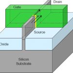
Additional process steps are required to introduce impurities of the appropriate type below the fin to provide a punchthrough stop (PTS), ensuring there is no direct current path between drain and source that is not electrostatically controlled by the gate input.
The dielectric between pedestals that remains after etch-back serves as the field oxide, as denoted in Figure 3. The gate material traversing between parallel fins is well-separated from the substrate, minimizing the Cgx parasitic capacitance.
The uniformity and control of the final fin dimensions are important process characteristics, for both the fin thickness and fin corner profiles. (The profile of the pedestal below the fin is less critical, and may be quite tapered, as shown in Figure 3.) Tolerances in the fin thickness arise from variations in the vertical, anisotropic SIT silicon etch. The fin thickness at the bottom is also dependent upon the uniformity of the etch-back – the goal is to minimize any dielectric “foot” remaining at the bottom of the fin.
As will be discussed in the next series installment, variations in t_fin have significant impact upon the transistor model. The top corner profiles also have an impact upon the transistor behavior, as the electric fields from the gate to the silicon fin are concentrated in this region, originating from both the sidewall and top gate materials.
Gate patterning follows conventional photolithographic steps, although the recent introduction of metal gate materials has certainly added to the complexity, especially as the gate must now traverse conformally over parallel fins. As with a planar FET technology, the gate length is the ‘critical dimension’ that is typically quoted as the basis for the process node – e.g., 20nm.
In contrast to planar FET technologies, providing multiple FinFET threshold voltage (Vt) offerings requires significant additional process engineering. The threshold of any FET is a function of the workfunction potential differences between the gate, dielectric, and silicon substrate interfaces. In planar FET’s, multiple Vt offerings are readily provided by shallow (masked) impurity implants into the substrate prior to gate deposition, adjusting the workfunction potential between dielectric and channel. However, the variation in the (very small) dosage of impurities introduced in the planar channel results in significant Vt variation, due to ‘random dopant fluctuation’ (RDF).
With FinFET’s, there is ongoing process development to provide different metal gate compositions (and thus, metal-to-dielectric workfunctions) as the preferred method for Vt adjust. The advantage of using multiple gate metals will be to reduce the RDF source of Vt variation substantially, as compared to implanting a (very, very small) impurity dosage into the fin volume. The disadvantage is the additional process complexity and cost of providing multiple metal gate compositions.
Another key FinFET process technology development is the fabrication of the source/drain regions. As was mentioned in the first series installment, the silicon fin is effectively undoped. Although advantageous for the device characteristics, the undoped fin results in high series resistance outside the transistor channel, which would otherwise negate the drive current benefits of the FinFET topology.
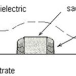
To reduce the Rs and Rd parasitics, a spacer oxide is deposited on the FinFET gate sidewalls, in the same manner as sidewalls were patterned earlier for SIT fin etching. To increase the volume of the source/drain, a ‘silicon epitaxy growth’ (SEG) step is used. The exposed S/D regions of the original fin serve as the “seed” for epitaxial growth, separated from the FinFET gate by the sidewall spacer. Figure 4 shows the source/drain cross-section after the SEG step.
Figure 4. Cross section of source/drain region, after epitaxial growth. Original fin is in blue — note the faceted growth volume. The current density in the S/D past the device channel to the silicide top is very non-uniform. From Kawasaki, et al, IEDM 2009, p. 289-292.
The incorporation of impurities of the appropriate type (for nFET or pFET) during epitaxial growth reduces the S/D resistivity to a more tolerable level. The resistivity is further reduced by silicidation of the top of the S/D region. In the case of pFET’s, the incorporation of a small % of Ge during this epitaxy step transfers silicon crystal stress to the channel, increasing hole carrier mobility significantly.
Raised S/D epitaxy has been used to reduce Rs/Rd for planar FET’s, as well. However, there are a couple of interesting characteristics to FinFET S/D process engineering, due to the nature of the exposed fin S/D nodes, compared to a planar surface.
The epitaxial growth from the exposed crystalline surface of the silicon fin results in a “faceted” volume for the S/D regions. Depending upon the fin spacing and the amount of epitaxial growth, the S/D regions of parallel fins could remain isolated, or could potentially “merge” into a continuous volume. The topography of the top surface for subsequent metallization coverage is very uneven. The current distribution in the S/D nodes outside the channel (and thus, the effective Rs and Rd) is quite complex.
FinFET’s could be fabricated with either a HKMG ‘gate-first’ or a ‘gate-last’ process, although gate-last is likely to be the prevalent option. In a gate-last sequence, a dummy polysilicon gate is initially patterned and used for S/D formation, then the gate is removed and the replacement metal gate composition is patterned.
FinFET’s also require a unique process step after gate patterning and S/D node formation, to suitably fill the three-dimensional “grid” of parallel fins and series gates with a robust (low K) dielectric material.
Contacts to the S/D (and gate) will leverage the local interconnect metallization layer that has recently been added for planar 20nm technologies.
The next installment of this series will discuss some of the unique FinFET transistor modeling requirements.
Also read: Introduction to FinFET Technology Part III