

Joe Sawicki is the VP and General Manager at Mentor Graphics for the Design-to-Silicon Division where the Calibre product line is developed. We met today in Wilsonville, Oregon to review the challenges in IC design, processing and manufacturing.

I first met Joe while at Silicon Compilers in the 90’s and have seen him grow into a variety of roles from applications to marketing to management. One of his hallmarks is the ability to respond to your email typically within a business day and his replies are succinct and to the point.

Q: What does Design to Silicon mean?
A: Design To Silicon is the action of going from the abstract design to the real manufacturing side of ICs.
Q: What are some of the technology challenges that you see for IC design and processing?
A: With the scaling complexity for each new node there is a doubling of transistor counts which puts pressure on doing physical verification (DRC, LVS, OPC, RET), so we still have to complete verification in a reasonable time like 6 hours. To keep up the scaling trends we see emerging technologies like EUV (Extreme Ultra Violet lithography) that may be ready by the 14nm node.
Source: Wikipedia
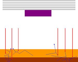
Image formation mechanism in EUV lithography. Top:EUV multilayer and absorber (purple) constituting mask pattern for imaging a line. Bottom: EUV radiation (red) reflected from the mask pattern is absorbed in the resist (amber) and substrate (brown), producing photoelectrons and secondary electrons (blue). These electrons increase the extent of chemical reactions in the resist. A secondary electron pattern that is random in nature is superimposed on the optical image. The unwanted secondary electron exposure results in loss of resolution, observable line edge roughness and linewidth variation.
Q: Why hasn’t EUV become production ready sooner?
A: EUV promises have not been production ready because of mask defects and power issues. Some researchers are saying that traditional scaling may stop at the 8nm node.
Q: How can IC technology progress if straight scaling is becoming less viable?
A: Many fabs will adopt FinFETS like Intel is now using, it really is less about patterning and more about channel efficiency at the 14nm and 11nm nodes.
Directed self-assembly (DSA) is one approach for extending optical lithography. It’s a technology that uses traditionally defined substrates with self-assembled polymers. The research papers from the SPIE conference have shown how lithography can be used to define the surface of silicon then block co-polymers are added that actually assemble themselves into predictable arrays that follow the defined pattern.
Carbon nano-technology is another candidate to replace silicon.
IBM paved the way for commercialization of carbon-based semiconductor chips with its dual-gate bi-layer graphene field-effect transistors.
The next few nodes are very challenging. We need manufacturing info going back into design so that we don’t have to be litho engineers when designing.
Q: How is Mentor involved with Direct Write to Wafer (DWW) technology?
A: We’ve joined a research consortia in Europe, and it’s a potential solution to enable scaling. It has similar challenges to EUV (although EUV has more research dollars behind it). Fundamentally we’re translating polygons from the IC layers directly into beam formations, and that is computationally intense.
EUV was talked about 4 years ago as if it had no needs for OPC, however at the 14nm node it will require OPC (correct for flare, some proximity effects, lots of effects to distort patterns).
Q: What approaches are used to speed up verification jobs?
A: With Computational lithography it makes sense to use a GPU to help speed up FFT calculations, maybe non-homogenous computing. Mentor did partner with Mercury Computer several years ago and that used the Cell Broadband engine to speed up the calculations. For 20nm and 28nm we still see x86 type CPUS being used for computations.
Q: Over the years how have DRC/LVS run times improved?
A: As an example in 1997 we ran a benchmark on an IC design that took 16 hours to verify and today that same task using distributed processing completes in 5 minutes, thanks in part to new algorithms and compute approach.
Q: Calibre started out in the mid 90’s, how has it changed?
A: If you compared Calibre today with what it was in 1997 you’d see mostly new code, entirely re-written to maintain technical leadership.
Q: Are patents used much to protect your EDA software?
A: Patents are not that relevant for EDA software, they are mostly defensive used defensively.
Q: To what do you contribute the sustained success with the Calibre product line?
A: Our engineering approach is very focused and different from other software companies because we give developers the freedom to innovate. Our developers are very close to the top customers, plus we have many visits. TSMC is a close partner and we have a good sized engineering force in Taiwan to be near TSMC. With Calibre PERC we’re planning some new and unforeseen uses after recent customer visits.
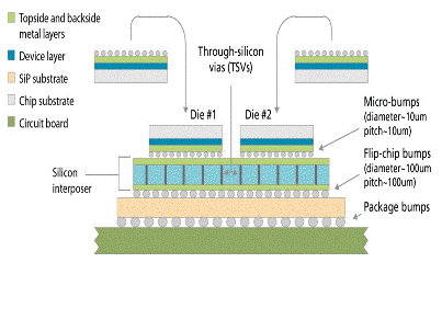
Q: 3D is the buzzword of the year for IC packaging. What do you see emerging here?
A: Die stacking could take over from pure transistor scaling possibly but not in the short term because scaling will continue to dominate. Chips like a GPU could benefit from 3D design. Memory stacks (i.e. Micron, IBM) looks compelling. Processor + Memory is promising. Mobile apps – will use 3D only if cost and power savings are there.
Q: What do you see with 2.5D and the use of silicon interposers?
A: 2.5D is interesting for RF+Analog+Digital (Silicon Interposer). How to validate and verify this is another big challenge on the testing side. Companies are trying to drive down the average cost per function. Physical verification and LVS for 2.5D and the design flow is in place today.
Q: For FinFET technology is there anything new required in Calibre?
A: Not really because the architecture was defined to allow device patterns to identify any type of device, even FinFET.
Q: Do 3D transistors like FinFET have any unique design challenges?
A: Yes, the 3D construction requires more accurate extraction to create netlists for SPICE, so you have to use a fast 3D field solver on FinFETs.
Q: How do test and design work with 3D packaging?
A: We’re combining test with Calibre and building up the basics of Known Good Die (KGD). With 3D stacks it costs to much to throw away a bad die. We’ve extend the fault models to more than just cell pin stuck-at, including cell internal stuck-at, improving coverage. For the automotive market having a lower Defect Per Million (DPM) is a big deal. On a large die lowering defects to under 500 DPM is an important goal. 3D parts need to be tested in a better way using techniques like BIST for logic and memory. We believe that using test to tie in with yield learning and DFM has a benefit. There is lots of hidden data in the individual fail logs, so if you collect that data and statistically determine what is failing inside each part after diagnostics then it can be used for analyzing low yields. Our goal is cell aware Known Good Die, that is the ability to define fault models within the cells, not jast at the boundaries. With this apprach we can even improve the economics of old nodes like 90nm to help find and improve yield issues for companies.
Q: Where are your Calibre products developed?
A: Our development is mostly domestic in Wilsonville and San Jose. Through various acquisitions and growth we also have developers in Taiwan, Armenia (Ponte – Critical Area Analysis), Egypt, Grenoble, Moscow, Poland and Hamburg.
Q: Earlier in the year Carl Icahn managed to get three new board members elected at Mentor. How has that affected your division?
A: There’s been no real impact on how the D2S division is run. We are all trying to maximize our development and sales efficiency.
Q: What are your interests outside of work?
A: I have a love of photography, both for candid family photos and landscape photography. I do editing in Photoshop and have an Epson 4800 printer with pigment based inks to create my own prints. I like to shoot with either a Canon DSLR or a Panasonic GF1.

We also have an 8 year-old son that is being raised to speak in English, Italian and Mandarin Chinese.


Comments
There are no comments yet.
You must register or log in to view/post comments.