 The 40[SUP]th[/SUP] SPIE Advanced Lithography conference will be at the San Jose Convention Center 22-26 February. Over the past few years, this conference has grown in scope to include emerging patterning technologies, like directed self-assembly (DSA) and design-process-technology co-optimization.
Underlying all the presentations, posters, panels, and hallway chatter are common goals and challenges: keep the fabs working and yields high, while controlling cost and turn-around time as the law of physics work against you.
One key component of managing modern manufacturing is computational lithography, which includes:
- Optical proximity correction (OPC) and resolution enhancement technology (RET) software and methodologies that achieve the maximum possible lithography entitlement
- Software, applications, and methodologies that allow foundries to increase their productivity and thus reduce development cycle times and associated costs
- Manage the post-tapeout flow
 You will see plenty of this type of technology presented at the SPIE Lithography conference. There are papers on incorporating DSA in multipatterning, analyzing litho hotspots with pattern matching software, enhancing local printability in sub-14nm nodes, model-based mask preparation, new modeling of 3D effects, and managing OPC jobs for better productivity and use of resources. These technologies help maintain reasonable turnaround times for the entire post-tapeout flow and manage foundry production costs.
The importance of modeling
I talked to John Sturtevant, the director of modeling and verification solutions at Mentor Graphics about some of the hot topics in computational lithography. He said that there are significant modeling challenges associated with the 14 and 10 nm manufacturing process nodes, particularly the need for accurate and fast simulation of three-dimensional phenomena associated with the mask, wafer, and resist.
“3D EMF effects associated with mask topography have been effectively modeled for many years,” Sturtevant said, “and to support 14 nm, we added refinement of edge to edge crosstalk signals in DDM.” This enhancement leads to significantly better matching to rigorous simulation with very little runtime impact. Using the crosstalk DDM library results in better wafer fitness, especially when the mask absorber sidewall is optimized in conjunction with mask bias, he said.
Sturtevant points out that formerly “non-critical” implant layers now pose a significant OPC challenge. Underlayer topography models, which capture the complex array of wafer topography effects, have been deployed for 14 nm. These models are being expanded to better represent the impact of active FinFETs and the results for pre- and post-poly layer implant models have been excellent.
There is also new focus on the photoresist model. The 14 and 10 nm nodes feature extensive use of negative-tone develop (NTD) resist processes for the patterning of metal and via layers, due to the intrinsic aerial image advantage of a bright field mask. These NTD resist processes have unique shrinkage and develop rate properties compared to the traditional positive-tone processes. Sturtevant says Mentor has modified the CM1 model to support new NTD-specific modelforms, with a 40-55% improved accuracy in predicting wafer results. They have also rolled out improvements in the prediction of resist toploss and scumming as well as SRAF printing for both PTD and NTD cases.
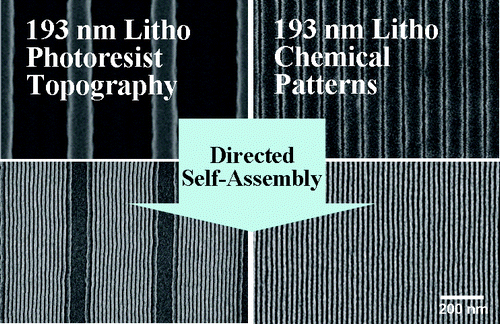
DSA is now on the near horizon, and compact models predicting the assembly of vias inside of guiding patterns are already available to assist in development efforts. An important consideration for these models is to ensure the proper 3D formation of the vias. You can expect to hear a lot about DSA, and computational platforms for DSA, at SPIE Advanced Lithography this year.
So if you are involved in design for manufacturing or post-tapeout engineering, don’t miss SPIE this year from February 22-26, 2015 at the San Jose Convention Center.
Share this post via:


Comments
There are no comments yet.
You must register or log in to view/post comments.